This thread has been locked.

If you have a related question, please click the "Ask a related question" button in the top right corner. The newly created question will be automatically linked to this question.

TPS57160-Q1 Instability with high input voltage

Other Parts Discussed in Thread: TPS57160-Q1

Hello,

I just finished building a board using the TPS57160-Q1 buck converter and as soon as the input voltage gets over about 30-35 Volts (We have an input voltage varying between 25V and 40V), we experience audible ringing of the buck converter and a kind of instability.

The needed output voltage is 5V, but with an input voltage of 35V and a load of 50-200mA @ 5V, we experience a high frequency toggling of the output voltage between 4V and 6V. The ringing/instability starts at about 20V and gets gradually worse with higher voltage. The component values were chosen by using the Webench-Designer: http://webench.ti.com/webench5/power/webench5.cgi?base_pn=TPS57160-Q1&Flavor=NA&AppType=None&topology=&optFactor=1&VinMin=10.8&VinMax=44&O1I=0.9&O1V=5&op_TA=30&application=POWER&origin=pf_panel

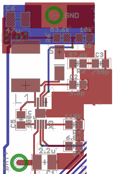
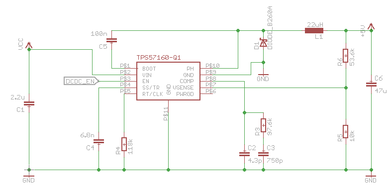
I would greatly appreciate if you could take a look at this design. I have attached both the schematic and the (hopefully readable) part of the PCB layout.

Thank you very much in advance

  • Hello,

    I suspect that you may be having some issues with the duty cycle as it will change considerably if you increase your input voltage.

    I suggest the following:

    * Go through the  "Selecting the Switching Frequency (section: 8.3.12) in the datasheet and see whether you see something related to this topic.

    * Change the switching frequency to 400KHz or something and see whether you still see the issue.

    * your input capacitor is 2.2uF and i don't know its voltage derating and this can significanty derate as Vin is increased. So increase this capacitor to 10uF/20uF or so with at least 50V rating.

    * Also noticed that your Cin is placed bit away from output capacitor and not sharing direct GND connections with output capacitor and recirculating diode. Can you please go through "Figure 65. PCB Layout Example" in the datasheet and try to make place this capacitor GND close to Cout/D1 GND and see the effect?

    * If you still have issues, please send me some oscilloscope plots showing, Vin, Vout, PH node waveform and if possible input current.

    Regards,

    Murthy

  • Thank you very much for the quick reply. I will try the suggestions and update this post with the results ASAP!
  • Ok, so far the things I've tried:

    * The switching frequency was really on the higher side. I tried to change it to 400kHz as you said, unfortunately to no avail (see plots later)

    * The voltage rating of my 2.2uF cap was 100V, so it should technically have sufficed (even with derating). Still, I tried to add another electrolytic cap in parallel to the ceramic one of the original configuration - still no noteworthy change in the output.

    * My CIn and COut are in fact a bit apart. Does this really have such a great impact? Is there any way I could test/simulate if this is the case without getting another board manufactured? Concerning the missing GND connections: they are there, I mistakenly clipped one of those in the layout I uploaded. The rightmost lone connection goes from C3 to GND (of the diode)

    * I tried increasing the capacitance of the output capacitor from 47uF with a voltage rating of 10V (ceramic) by adding a 57uF cap (Rating: 63V) in parallel to it. Still, output not really changed)

    * I tried changing the frequency compensation components (COMP pin) to a (at least according to webench) more robust combination: R3=130k, C3=470p, C2=4.3p. Did not help either.

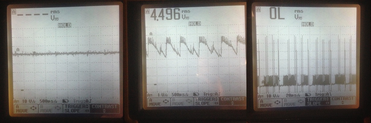
    Here the plots - please excuse the quality. I only had access to a mobile scopemeter today.

    Original configuration. From left to right: Vin, Vout (10mA load), Vout (250mA load), PH pin under load

    Modified configuration (As outlined above: larger input cap, 400kHz switching frequency, "robust" comp pin components). From left to right: Vin, Vout (10mA load), Vout (250mA load), PH pin

    Modified configuration 2 (larger input capacitor, "robust" comp pin components, original switching frequency: 950kHz). From left to right: Vin, Vout (250mA load), PH pin under load

    Now that I have modified not only the input and output capacitors, but also varied the switching frequency over the whole spectrum and changed the components connected to the COMP pin, I tend to think that the culprit is the placement of the capacitors. I would greatly appreciate any comments on that - maybe you can see more based on the plots above. Thank you in advance!

  • Hello,

    With 400KHz switching frequency, i can see that there is some improvement, but still , switch node does not seem to be switching continuously and still some missing pulses.

    With 900KHz switching frequency, regulator is doing some pulse skipping and poor ripple performance is expected.

    Due to some measurement issues, you may see little more ripple and see the below link to do the correct ripple measurements.

    https://e2e.ti.com/support/power_management/simple_switcher/w/simple_switcher_wiki/2243.understanding-measuring-and-reducing-output-voltage-ripple


    Cin, Cout and diode placement can make considerable difference and to confirm this, can you solder your 2.2uF input capacitor very close to device pin and

    short its GND connection directly to diode GND with thick wire and see whether this helps?

    * your load current may be still less and device may be in DCM mode of operation. you can check this by increasing the load current and monitoring switch signal. you have to

    to see the switch signal with may be around 5us/div scope resolution to see this signal closely.

    * Also try reducing the inductor value to 10uH or so? just to check it.

    Regards,

    Murthy

  • Hello,

    thanks again for the support.

    I will redo the measurements as soon as possible.

    I now tried manually soldering the components to closer positions. The input capacitor was only 2mm away from the input pin, the cathode of the diode and the inductor only 1mm away from the PH pin of the controller. I had to use a 10mm wire from the GND of the input cap to the anode of the diode though. Should that be enough of loop reduction?

    Could it be that my load current is just too small? Shouldn't the controller also be stable with smaller load currents?

    I will try reducing the inductor value as well.

  • Hi,

    adding the input capacitor close to the device pin helped a bit or not? Your wiring should be good enough to check its effect.

    As i already specified in my previous post, i could be possible that you have less load and device is getting in to pulse skip or DCM mode and cause some issues.

    But you need to check these on your board to confirm these issues.

    Regards,

    Murthy

  • Oh sorry, I totally missed mentioning that. Unfortunately, the output voltage is still a sawtooth shaped voltage with a peak-to-valley voltage of about 1V. So unfortunately this didn't bring the effect I hoped either.