This thread has been locked.

If you have a related question, please click the "Ask a related question" button in the top right corner. The newly created question will be automatically linked to this question.

SM320C6727B: Asynchronous EMIF write hold time question and I/O dynamic voltage compatibility for the space qualified part.

Part Number: SM320C6727B
Other Parts Discussed in Thread: SMV320C6727B-SP,

  1. The Asynchronous EMIF bus has the following delays from pg. 49 on the datasheet, with signals having a min of 0 nS and max of 8 nS.  For the write hold timing if I consider the minimum delay for EM_CLK to EM_D being 0nS and maximum delay for EM_CLK rising to EM_WE being 8 nS I would have a negative hold margin considering the large difference between min and max.  I’m wondering if my interpretation of this timing diagram is incorrect and that actually there’s two clock cycles of positive margin for hold before the Data delays are considered?

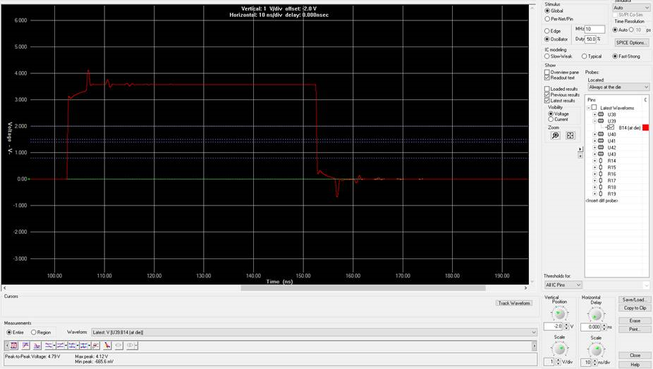
2. Looking at the waveform below I’m wondering if there’s an AC spec. that would be acceptable for exceeding the absolute Max/Min overshoot for the 3.3V digital I/O receivers.  As shown below the peak to peak voltage is 4.12V to -0.666V, which exceeds the datasheet spec of -0.3 to DVdd + 0.5V.  However the spike is only for brief period of time considering the period of the signal.  Would this be acceptable for this device and is there documentation for that?

  • Will,

    For #1, your thinking is on the right track but the top arrow between the table and the timing diagram is referencing the DQM byte write strobes, which are not used very often; and they would be expected to turn off at the same time as the WE strobe although used independently. Instead, you should reference the EM_D bus which is 3 lines lower in the timing diagram and shows EM_D being valid until the end of the HOLD period. The amount of extra hold time that you specify for the HOLD parameter does extend the hold time for EM_D after WE goes away. It is safe to make the assumption, as you are doing, using the max delay on WE compared with the min delay on EM_D, and then add the two extra cycles for the case shown (HOLD=2, A1CR.W_HOLD=1). In reality, the signal delays will never be at opposite extremes of the MIN/MAX range but for this device we do not have data to narrow that gap.

    By the way, you appear to be using the SM320C6727B-EP datasheet. The SMV320C6727B-SP datasheet (for the space qualified device you mentioned) has a different timing table with some changes from the -EP datasheet.

    I will need to let someone else comment on the overshoot/undershoot specification question in #2.

    Regards,
    RandyP
  • Thanks Randy.
    The clamp current in the absolute max ratings table indicates a +/- 20ma limit. This limit is intended to protect the ESD diodes from overstress. As long as you do not violate this, you will not overly stress the ESD structures.

    Your IBIS simulation looks a little odd though. The waveforms do not show traditional overshoot/undershoot damped signature.
    If you provide your loading and model used I can take a look at it. I suspect the IBIS model.

    However, I must note that I will be on vacation starting tomorrow until July 2nd. So, I will not be able to comment more until then.
    Regards,
    Wade