1. What is the purpose of using the BAV99 and the DLW31? Are they mandatory for HRM applications?
BAV99W switching diodes are primarily used as diode clamps. If you expect to see accidental higher voltages at the INN, INP, DETP and DETM lines, it is recommended to use clamp diodes to supply and ground to protect the AFE44xx. For battery operated systems this might not be necessary.
DLW31 are EMI suppression filters. In wearable systems with wireless capability, RF energy can attenuate the signals on the INN and INP channels. It is recommended to use the common mode choke coils to suppress common mode noise.
2. Is it possible to use only one led or it is compulsory to use two LEDs in different bands?
The AFE44xx family of devices supports two LEDs for Pulse Oximetry application. For HRM application, you can use only 1 LED with AFE44xx.
3. Recommendations of LEDs and Photodiodes tested with AFE44xx
|
Part number |
Mfr. |
Type |
|
SFH7050 |
OSRAM |
Integrated triple LEDs (Red, IR and Green) and photodiode |
|
NJL5310R |
NJRC |
Integrated dual Green LEDs and photodiode |
|
NJL5513R |
NJRC |
Integrated four LEDs (Red, IR and 2 Green) and photodiode |
|
DCM03 |
APM Korea |
Integrated dual emitter and photodiode |
|
APL3015MGC-F01 |
Kingbright |
Green Led |
|
IR17-21C/TR8 |
Everlight |
IR Led |
|
QSB34CGR |
Fairchild |
Photodiode |
4. What is the recommended LED_DRV_SUP voltage (AFE4400, AFE4490 and AFE4403)?
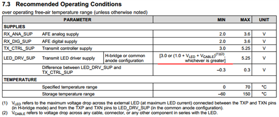
Depending on the type of LED (green, red or IR) (Vfb of the LED) connected between TXN and TXP and the TX_REF voltage, the LED_DRV_SUP might require to be high as 5V. The datasheet mentions the recommended operating conditions for LED_DRV_SUP (see below)
5. Does LED_DRV_SUP pin require a bulk cap?
The device can draw high switching currents from LED_DRV_SUP pin. It is recommended to have a bulk cap (atleast 10uF recommended) connected to LED_DRV_SUP pin.
6. What are the layout guidelines for INN, INP and VCM signal of AFE44x0?
Route the Receive signals (INN and INP) differentially with tight coupling at approximately the same length. Use VCM signal to shield the INP and INN traces. VCM signal is intended to guard the INN and INP traces from common mode noise (as shown below). VCM is a reference voltage that is generated internally and is used to bias the input common mode of the TIA. By shielding the traces of the photodiode connections to the INP and INN inputs with VCM, any leakage current created by the impedance between INP/INN traces and GND line can be prevented.
7. AFE44xx sign of life after power-up
7a. For AFE4400, AFE4490, AFE4403
After ensuring the AFE power supplies are fine and setting RESETZ and AFE_PDNZ to logic high, you should measure the following:
a) 0.75V on TX_REF pin (pin#9) for AFE4490.*
b) 1V on BG pin (pin#7)
c) 0.9V on VCM pin (pin#4)
d) 4MHz clock on CLKOUT pin (pin#30) - assuming there is an external 8MHz crystal on XIN-XOUT pins.
* Note: After programming the registers to the default values in AFE4400, TX_REF pin will read 0.5V.
7b. For AFE4404
After powering up the AFE,
1. issue a reset to the AFE by applying a 25-µs to 50-µs duration active low pulse on the RESETZ pin.
2. the AFE has a CLK pin. Depending on the clock mode determined for the application, apply an external 4MHz - 60MHz clock (default mode after reset) on the CLK pin or program the OSC_ENABLE bit for selecting the internal oscillator clock. In external clock mode, a programmable internal division ratio between 1 to 12 must be set so that the divided clock is between 4 MHz to 6 MHz.
3. configure the AFE for LED on/off, sampling, conversion and ADC reset timing edges, LED currents, TIA gain and Cf setting and PRP_COUNT.
4. monitor the ADC_RDY pin. The periodicity of the ADC_RDY pulses will occur at the pulse repetition frequency configured.
8. How does AFE44xx SPI (AFE4400, AFE4490, AFE4403) timing waveform look like?
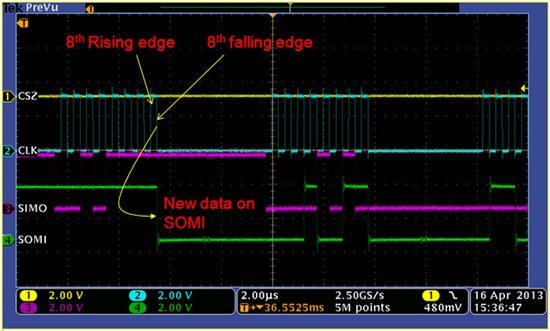
The MCU serial port must be configured to latch serial data out on falling edge, such that AFE44xx can clock data in on the rising edge. Likewise, the AFE44xx will shift data out on the falling edge so MCU can clock data in on the rising edge.
9. Can you provide the initialization sequence of AFE4400, AFE4490, AFE4403?
A possible initialization sequence may be:
i. Set SW_RST bit – resets all registers to default values.
ii. Set DIAG_EN bit – Enable diagnostic mode
iii. Set SPI_READ bit – SPI read is enabled
iv. Read DIAG register – Check for fault flags
v. Reset SPI_READ bit – SPI read is disabled
vi. Configure AFE
- Write to Timing Control registers (0x01 – 0x1D)
- Write to other control registers (0x1E, 0x20 – 0x23)
vii. Set SPI_READ bit – SPI read is enable.
viii. Read ADC registers (0x2A – 0x2F) – from host controller based on ADC_RDY signal interrupt
10. Why is the 22-bit ADC full scale code not 0x1FFFFF?
The 22-bit ADC data is not full scale (0x1FFFFF) due to the radix 2 division for ADC averaging.
11. What is the recommended TIA and ADC operating range?
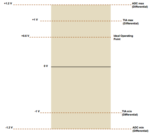
The TIA has an operating range of ±1 V, and the ADC has an input full-scale range of ±1.2 V (the extra margin is to prevent the ADC from saturating while operating the TIA at the fullest output range). Furthermore, because the PPG signal is one-sided, only one half of the full-scale is used. TI recommends operating the device at a dc level that is not more than 50% to 60% of the ADC full-scale. The margin allows for sudden changes in the signal level that might saturate the signal chain if operating too close to full-scale. Signal levels in TIA and ADC are shown in figure below.
12. How does second stage ambient cancellation DAC work?
The second stage gain and ambient DC cancellation block does not cancel the DC component of the pleth signal. It can be used to offset the DC due to ambient and amplify the pleth signal (DC + AC).
Let us assume that at the TIA output, the DC of pleth signal with ambient is around 1.1V and AC component is 10mV and the ambient DC signal is 0.9V.
With Ambient subtraction of 4uA, the ambient DC is reduced to 0.1V and the DC of pleth signal is around 0.3V and the AC component is still 10mV.
Now with stage2 gain of 3, the ambient DC will be 0.3V and pleth DC will be 0.9V and the AC component will be 30mV.
Below is an illustration of ambient cancellation and stage 2 gain.
The cancellation voltage is 2 x Ri x Icancel where Ri = 100K.
With 4uA of cancellation current, then the cancellation voltage will be 0.8V.
With the digital ambient cancellation and stage 2 gain, it enables adaptation to fast changing ambient light. The example above was to illustrate the ambient cancellation and stage 2 gain feature. The TIA gain could range from 10K to 1M.
At higher TIA gains, when the ambient light is too high, decreasing the TIA gain not only reduces the DC component of the ambient signal but also reduces the DC and AC components of the pleth signal. So using the ambient cancellation and stage 2 gain, you can offset the DC due to ambient and amplify the pleth signal (DC + AC).
At lower TIA gains, when the ambient light is too high, you can quite easily observe the benefit from the ambient cancellation and stage 2 gain.
13. Is there a recommended way to AC couple the input to the AFE44xx?
No the AC component of the pleth signal cannot be isolated from the DC component by AC coupling the inputs to the AFE4490. This is because the LED is not continuously on but pulsed during the LED and LED ambient phases. That is, the photocurrent appears as pulses at the input of the TIA. Therefore the signal input to the TIA has high bandwidth. The TIA is also designed to have high bandwidth to be able to pass these pulses (I-V output pulses in the attached image). The sample and hold circuit (RC filter) is switched on only during the particular phase (LED and LED ambient phases). So it only sees the slow moving signal and not the pulse transient.
With the 22-bit ADC and the range of gain settings, you can measure both the AC and DC component without saturating the signal chain.
14. What does the 18 byte data information of 6 channels correspond to?
The data from each channel comes in 3 byte each, in this order, LED2, LED2Ambient, LED1, LED1Ambient, LED2 – LED2Ambient, LED1 – LED1Ambient.
Divide the data into six equal groups each consisting of 3 bytes. Then arrange the data in order (MSB first). Convert the hexadecimal to decimal to get channel code.
15. How to convert ADC results code to voltage?
The ADC volts to codes conversion formula is:
ADC data (volts) = (ADC codes in two's complement format * Vref ) / 2^21
where Vref = 1.2V
16. Can you please explain the averaging module in more detail? Is this a moving average filter? Or does this module capture and hold the voltage and then average multiple samples of that voltage?
Enabling averaging causes the ADC to convert the voltage sampled by the switched RC filter multiple times to reduce the ADC noise. The sampling is done once (across the capacitance of the switched R-C filter) and the same sampled voltage can be converted multiple times by the ADC (each conversion taking 50 us).
17. Can I know where TI has implemented the band pass filter and where actual filtering of raw data is taking place. Is it in Labview or on microcontroller?
The band pass filter was implemented in LabVIEW. The filter is a 3rd order Butterworth band pass filter between 0.5 and 2.5Hz.
18. What I need to do to get the HR signal from ADC volts( values got after converting ADC codes)?
In the filtered PPG data, the number of peaks correspond to the heartbeat rate.
There are several techniques to calculate the heart rate.
One technique is to calculate the heart beats per minute using a three beat average. First detect the presence of beats by comparing the outputs against a set threshold. Once you detect three beats, the heartbeat rate can be calculated as follows:
Heart rate per minute = sampling frequency (PRF) * 60 * 3 / number of samples in 3 beats
19. What are the careabouts to connect one of three photodiodes to the AFE44xx? Is it possible to use an analog switch/multiplexer to bring the signals into the TIA? Or will this compromise the accuracy of the system? Are there recommended switch/mux parts for this type of application?
The bias for the PD is set by the TIA through negative feedback. For AFE44xx, the TIA sets the PD to a zero differential bias. This bias is essential to ensure the PD operates with a predictable sensitivity.
When you disconnect a PD from the TIA through an external switch, there is no longer any mechanism of setting the PD bias. So the PD bias can drift.
When it is reconnected to the TIA, there will be a transient behavior associated with the TIA trying to get the PD back to zero bias. The time constant associated with this transient would be 2*Rf*Cin where Rf is the TIA gain and Cin is the differential capacitance of the PD.
So there are two things to analyze before doing something like this:
1. Make sure the PD voltage in open circuit does not drift to too high a value that goes out of bounds of the AFE44xx input pins.
2. Give sufficient time for the PD bias to settle after reconnecting it before the sampling is done.
We do not have any recommended switch parts.
20. What are the considerations in interfacing an optical source with AFE44xx?
Following points should be considered while interfacing optical source with AFE4404/AFE4490.
1) LED Driver is a constant current source between TX pin and GND. Current supplied as well as ON time of the LED Driver is programmable using register settings.
2) There is a limit in current supplied by LED Driver. In AFE4404, its 50mA (with ILED_2X = 0) and 100mA ( with ILED_2X = 1). At any point, the optical source should not draw current more than this limit.
3) Forward bias voltage of optical source should be such that, voltage at TX pin meets the headroom requirement of AFE4404/AFE4490.
4) Maximum current supplied by LED Driver can have accuracy of +/- 15%. This might effect the threshold current of source.


