This thread has been locked.

If you have a related question, please click the "Ask a related question" button in the top right corner. The newly created question will be automatically linked to this question.

ADS5263 16-Bit mode Full-Scale Input question

Other Parts Discussed in Thread: ADS5263

Hello,

I am trying to determine the full scale input for the 16-bit front end of the ADS5263. The part is advertised as having a 4vpp full scale input while utilizing the 16 bit front end. However the data sheet doesnt really make sense to me. It indicates that the device has a 2vpp full scale in both modes (this is my interpretation)

In the absoule max ratings (section 7.1 of the Rev. D datasheet) The "Voltage applied to analog input pins INP_A, INM_A, INP_B, INM_B" min= 0.3v and max=3.6v or AVDD + 0.3v. Now using these numbers you only have a 3.9vpp swing. I suppose you could look at the max AVDD voltage which = 3.9v and now you could potentially reach a 4.2vpp swing but these are absolute maximum ratings. Furthermore  in section 7.3 recomended operatiing conditions the maximum analog supply voltage AVDD = 3.6v with the nominal being 3.3v.

Another confusing section is the analog input section 9.1.1 (rev. D). Taken from the data sheet "The INxP and INxM pins must be externally biased around a common-mode voltage of 1.5 V, available on the VCM pin. For a full-scale differential input, each input pin INP, INM must swing symmetrically between VCM + 1 V and VCM – 1 V, resulting in a 4-Vpp differential input swing." The way I read this is that there is a +-1v swing resulting in a 2vpp swing. Am I missing something?

I called the technical support number and was told that the spec of 4vpp is correct but they couldnt tell me why and refered me to post on this forum to get an answer.

I've read through this data sheet quite a few times and I can't figure this out. Its possible that I'm missing something obious but thats why I'm here.

Thank you for your assistance on this matter!

Ethan

  • Traineef,

    I'm assigning your post to the correct applications engineer. He should respond soon.
  • Hello Ethan,

    Thank you for using ADS5263 device.

    We will look into your question very soon.

    Thank you very much.

    Best regards,

    Chen

  • Hi Ethan,

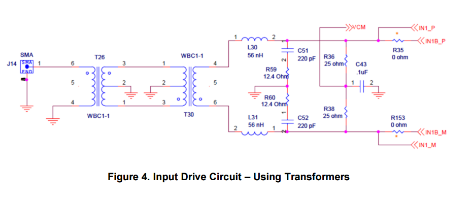
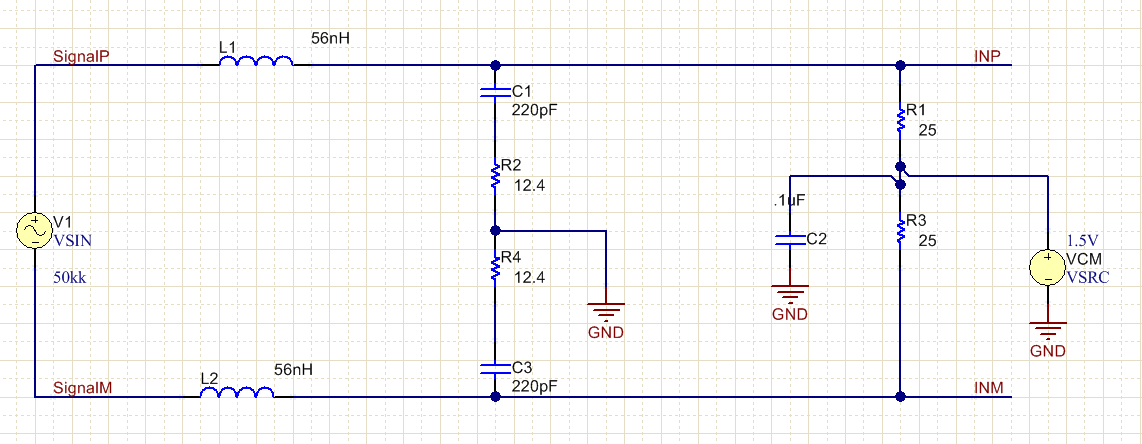
    Thank you for your question. Admittedly, the datasheet was a bit confusing on my first pass. However, since the input to the ADS5263 is a floating differential input, we need to keep in mind that the input voltage will not be required to swing past 2.5V on either ADC input pin, (INP & INM), with a full scale signal. Let me explain using a simplified version of our circuit in the ADS5263 EVM:

    Original EVM Circuit:

    Circuit with Isolation Removed for Simulation Purposes:

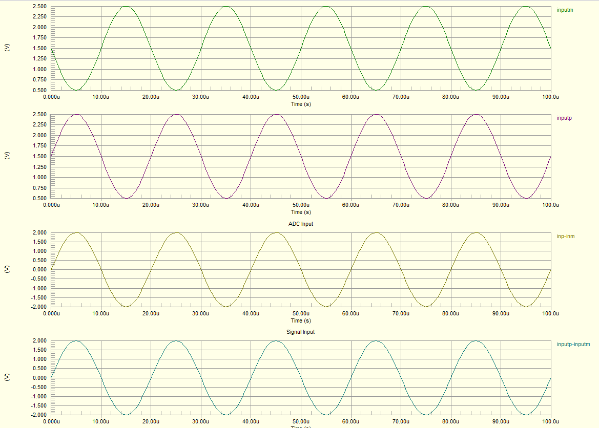
    In the fully differential topology, the input signal will drive the SignalP terminal to 2.5V and the SignalM to 0.5V on a high peak output. Likewise, the opposite will happen on the low peak output, achieving the full-scale 4V pk-pk input voltage shown in the datasheet. Below are the simulation outputs for the schematic above, (also 50kk -> 50MHz, I got lazy :) ):

    I've also included the Altium schematic, simulation outputs, and sim files I used below:

    ADS5263.7z

    If you have any other questions, feel free to post again. Thanks again for your question!

    Best Regards,

    Wilson

  • Hi Ethan,

    How are you?

    Please take a look at the attached file showing how the ADS5263 16-Bit

    input signal (analog) and output signal (digital) look like.

    Hope this is easy to understand.

    Thank you and best regards,

    ChenADS5263 16-Bit mode Full-Scale Input question.pdf2502.ADS5263 16-Bit mode Full-Scale Input question.pdf

  • Thank you Wilson and Chen for your answers. It makes perfect sense. I should have known better. For whatever reason I wasn’t thinking of it as differential full scale input. In my mind I was thinking of the output amplitude swing for each individual signal of the differential output of the ADC driver circuit. Of course this isn't the same as the differential voltage that is "seen" at the ADC input pins. Its very clear to me now.

    I suppose the "4 Vpp Full-Scale Input" in the features section on the first page of the data sheet is what tripped me up originally. However further down in the Characteristics and application information it is then referred to as "Differential Input Voltage". This is probably where I should have figured it out. Perhaps in the features section it should be listed as differential input swing as well.

    Thank you both again for your assistance on this.

    Best,

    Ethan

  • Any time! It's a pleasure to help.