This thread has been locked.

If you have a related question, please click the "Ask a related question" button in the top right corner. The newly created question will be automatically linked to this question.

DRV8840: PWM input to output timing

Part Number: DRV8840
Other Parts Discussed in Thread: DRV8844

Hello,

We use the DRV8840 to control a brushed motor without encoder feedback. If the motor does not reach the desired location in a set time the MCU generates an error. Because there is no motor feedback to control the speed we use a constant duty cycle to drive the motor. During development this approached worked well however we received some new DRV8840 parts with a different lot code that have different output characteristics. The output duty cycle is lower than previous lot codes and this causes the motor to move slower which generates a timing error. The datasheet doesn't discuss the tolerance of input duty cycle to output duty cycle. Is there a specification for this parameter? What is the recommended guidance for dealing with duty cycle tolerance?

Regards,

Michael

  • Hi Michael,

    In addition to the duty cycle at the input, the internal PWM circuitry can affect operation if the device is entering current regulation mode. You should be able to observe this by monitoring the output duty cycle with respect to the input duty cycle.

    Can you confirm the device is not entering current chopping as described in section 7.3.3 of the datasheet?

    You may need to increase the VREF, decrease the sense resistor, or adjust the I4:0 bits to avoid this condition.
  • Rick,
    Thanks for the reply. I used a 0.165 ohm current sense resistor and vref is supplied by the internal 3.3V regulator. Additionally, all of the current scaling pins are tied to V3P3OUT so the scaling is 100%. My calculations show this should give 4Amps output. The MCU sends a PWM to the ENBL
    input at 18% duty cycle. The motor current is around 100mA so the DRV8840 is not going into current regulation with a limit of 4A.

    Can you give guidance on how to account for all of the parameters that will affect the output? Does the command frequency not affect the internal PWM?

    Mike
  • Hi Mike,

    How are you measuring the motor current?

    You have accounted for most of the major parameters.

    The remaining ones are RDS(on), which can change with temperature and input deglitching on the ENABLE pin (see link e2e.ti.com/.../854065) .

    At 100mA, RDS(on) should not have much effect.
    The input deglitching could have an effect depending on the PWM frequency.

    What is the PWM input frequency?
  • Rick,

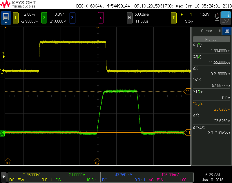
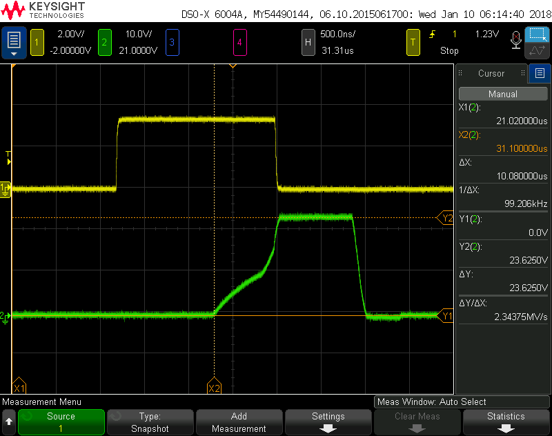
    I took some scope plots of the input PWM and output PWM from a good board and bad board. The output PWM of the bad board has a very long turn on rise time, around 770ns. The datasheet specs 300ns max. It appears there is something wrong with a few of these DRV8840. Below are images of good output (image 1) and bad output (image 2). Ch1 = input PWM Ch2 = DRV8840 pin 7.

    The input frequency is 100kHz.

  • Hi Mike,

    Would you please capture pin 5 or 10 of both boards in the image also?

    There does not appear to be any current in the coil of the bottom image, and you may be seeing the back EMF. I say this because the voltage in the upper image is less than 0V prior to the output rising, implying there is still current in the winding.

    Would you also confirm the DECAY pin is set to a logic low?
  • Rick,

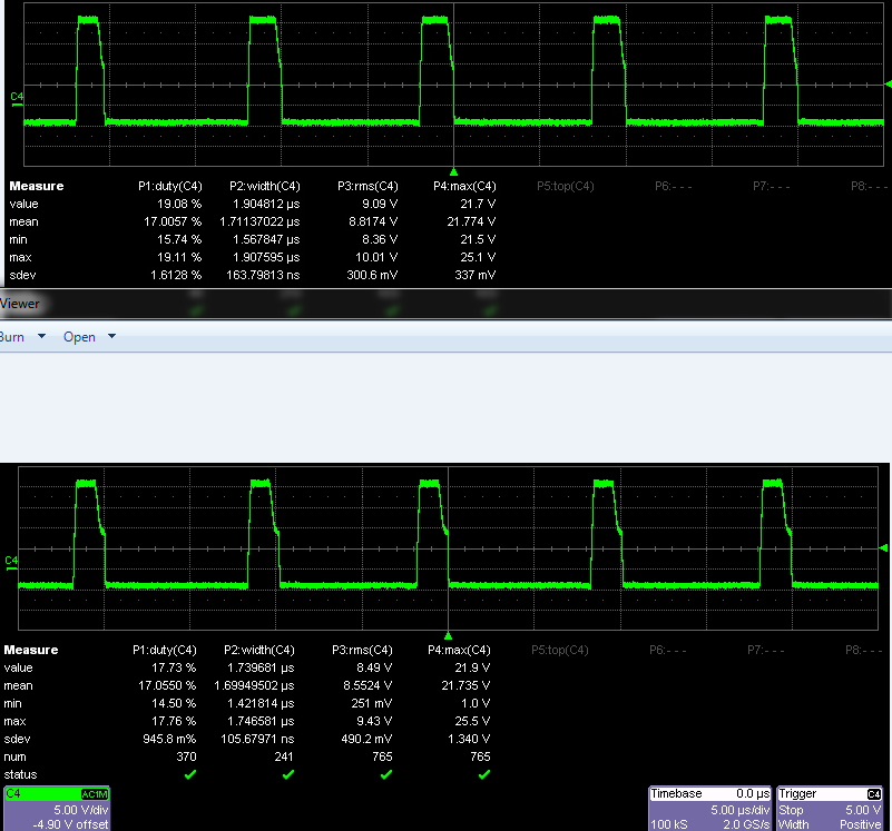
    Looks like my text got removed from the previous post. The top plot is pin 7 of a passing board the bottom plot show the same pin once the DRV8840 was replaced with a different lot code. The motor is not attached during this measurement. The pulse width is definitely different between lot code with the same system (PCB, motor and load). I'd like to know what to expect from part to part so I can adjust the software to account for the full range of tolerances. The datasheet only lists rise and fall times but there appears to be more at play here. Can you help?

    Thanks,

    Mike

  • Hi Mike,

    Let me look into this. I hope to have a response by Wednesday of next week.
  • Hi Rick,

    Any updates to share?

    Thanks,

    Mike

  • Hi Mike,

    Thank you for your patience. It appears there will be some variation due to internal synchronization of the inputs.

    On a device in our lab, the synchronization varies on both the positive edge and negative edge by approximately 300ns. Depending on voltage, temperature, and process, the variation could range from 240ns to 520ns.

    Since you are running at ~24V, the variation could range from 250ns to 420ns.
  • Hi Rick,

    Can you describe what you mean by synchronization variation?

    What I am taking this to mean is that after the enable pin goes high I can expect my output to start rising within 250ns to 420ns.  Similarly, once the enable pin goes low it will take 240ns to 520ns for the the output to begin to fall.  Is this the correct interpretation?

    My understanding, however, does not match the oscilloscope captures I've submitted before. The time from the rising edge of the enable to the rising edge of the output is about 1.2ms.

    Thanks

  • Hi Mike,

    Can you confirm you are seeing 1.2ms? Did you mean microseconds instead of milliseconds?

    There are two parts that affect the delay from input to output.

    The first is a deglitch circuit that prevents spurious noise propagating to the outputs. This can add ~800ns and varies from device to device also. Unfortunately I don't have any information on the variation of this part of the circuit available.

    The second part is a flip flop that is used to synchronize the signal for use by the digital core. This is the synchronization variation that I am referring to.
  • Rick,

    You are correct, I meant microseconds. 

    So there is a delay from input to output but that should not affect the duty cycle? Additionally, there is a synchronization circuit that add 250ns to 420ns. Is my understanding correct?

    Mike

  • Hi Mike,

    Yes, there is delay from input to output that should not affect the duty cycle. The synchronization circuit can affect the duty cycle and add 250ns to 420ns.

    If you need a device that preserves the duty cycle, please consider the DRV8844.