This thread has been locked.

If you have a related question, please click the "Ask a related question" button in the top right corner. The newly created question will be automatically linked to this question.

DRV8302: Problem about switching buck converter not working

Part Number: DRV8302
Other Parts Discussed in Thread: TPS54160, BOOSTXL-DRV8301, DRV8303, DRV8301

Dear comunity,

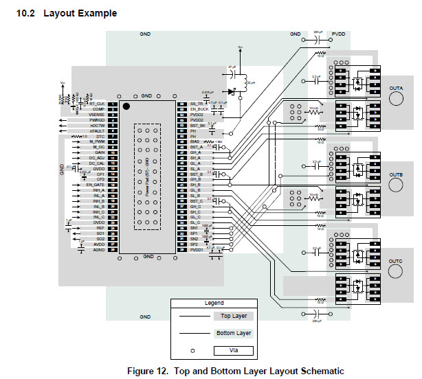
it seems I have problem with buck converter of DRV8302. I soldered it acording to this schematics:

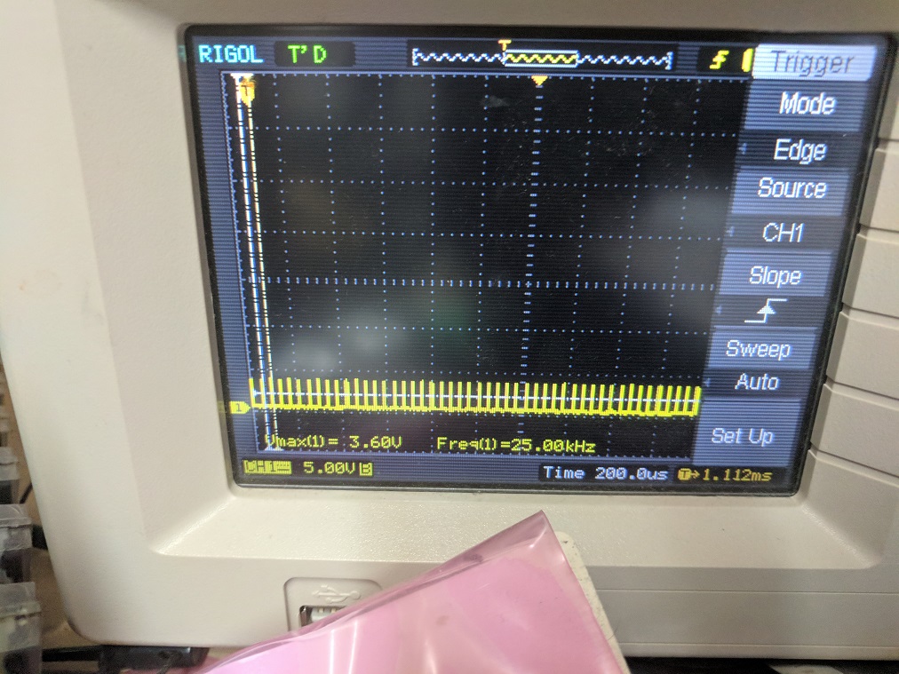
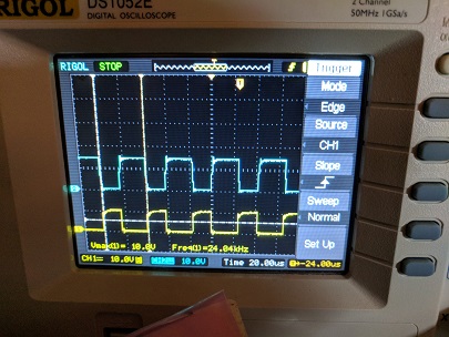
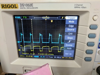
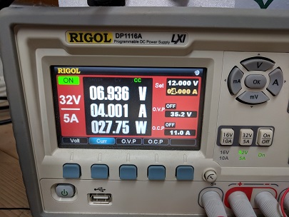
The voltage levels I get on relevant pins are as follows:

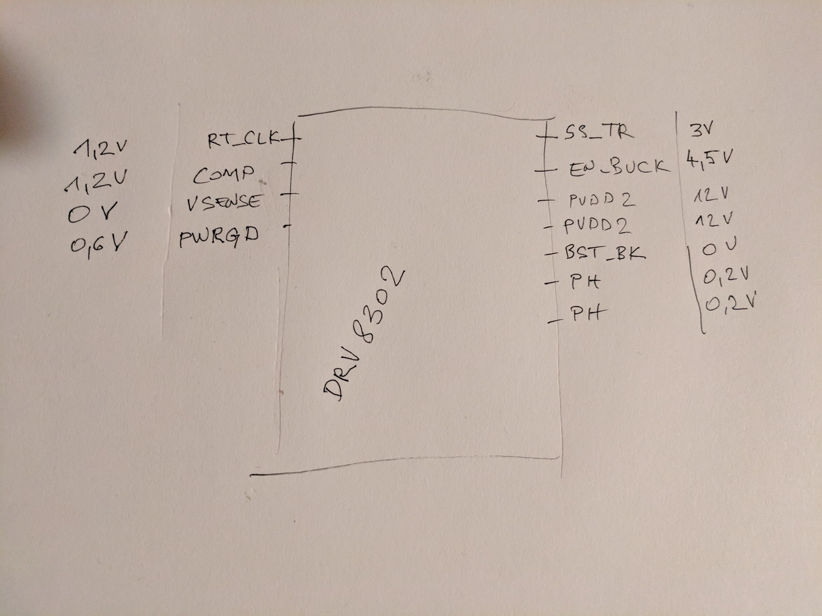
I am powering chip with 12V VDD.

(not)FAULT is pulled low - can you maybe suggest what else could I check to find what is causing this non desired operation.

Here is also pcb of board if needed.

  • Hi Zhivko,

    I don't think you can leave the SS_TR pin floating. I think you need to put a capacitor there.

    The TPS54160 is the buck we use in the DRV8302. That datasheet explains how to choose the capacitor on p18.
  • Hi James,

    acording to datasheet it seems you are are right - I will add this capacitor and report back. I hope I can keep thread open for this for a while.

    regards

  • Zhivko,

    I saw you also asked about nFAULT being held low. In this chip, the buck and the motor driver portions are not connected internally. When you fix the buck, there may still be an issue that triggers one of our protection features and holds nFAULT low. To debug why nFAULT pin is low, read through the section on protection features in the datasheet (7.3.4). You can probe your circuit during operation or startup to determine if the device sees any of these faults.
  • I just soldered 0.015uF as it is described in documentation for DRV8302 (8.2 Typical Application page 21) but that didn't helped - the same situation - I get same voltages as described above.

  • "When you fix the buck" ... yes - the question is how to fix it... Do you know how I can troubleshoot?

  • When I turn on 12V power supply BST_BK goes slowly (in 5second timeframe) to 5V, but PH stays all time at 0V.

    Also Vsense stays 0V all the time, but I see corect ss_tr and en lines as per TPS54160 datasheet:

  • Zhivko,

    I think your resistor divider on VSENSE might not have correct values. Double check section 8.3.8 in the TPS54160 datasheet for choosing those resistors.
  • I got this values copy paste from another project ( page 7) - now I recalculated as you suggest - and I get:

    R2=10kOhm

    R1=10kOhm * ((5-0.8)/0.8) = 52.5 kOhm
    I soldered those two - and plugged in 12V and no difference... :(
  • Zhivko,

    What is the purpose of D4 in your schematic? Can you remove it?

    Please review the Section 9.2.2 Detailed Design Procedures (p.31) in the TPS54160 datasheet. I skimmed this section, and I noticed that your bootstrap capacitor is twice the recommended value. This may cause the buck to not work correctly. If possible, you may want to try to make your setup identical to the design example, then change components one at a time until you have the performance you want.

    Also, you may want to use the oscilloscope in your debug process. This should help you check if the buck switches properly or if there is some other issue.
  • Hi James,

    Yes I can remove D4, and I did remove it.

    I changed capacitor between PH and BST to 100nF as per datasheet, restart plugging in 12V and no change - still nothing.

  • Hi Zhivko,

    You may have to use an oscilloscope to see which pins are working correctly, and which pins may not have the correct output signals. This will help you to focus your debugging activity.

    It is also possible this device was damaged with the initial incorrect components. Can you try another device or another board? I looked at your board picture again, and it looks like you hand soldered the IC and surrounding components. Before you try another device, make sure all the pads are free of old solder. When you solder the new device, use solder flux and make sure there are no solder bridges between pins.

    Also, I recommend finding the correct components to fit the pads on your board. It looks like many of your components are either too large or too small for the pads on the board. In a pinch this works, but sometimes it is difficult to solder good connections by hand in this case.

    If you are doing this for a prototype/proof of concept, I recommend using one of our EVMs (DRV8302-HC-C2-KIT or BOOSTXL-DRV8301) so you don't have to worry about board-level issues in the design.
  • Hi James,

    yes I use osciloscope all the time, the problem is knowing what is signals shout output what voltages this is why I documented voltage level in one of my first posts.

    But now I am posting all signals at the time of starting up drv8302 chip. Maybe you coud diagnose better (attached to word file)osciloscope_traces.docx

    Yes it could be the part is damaged - but I already resoldered another chip. Now I ordered 3 of them and I think this is cheaper than reference design that costs on farnell aprox 340€.

    Regarding bridges yes I use flux and i am making sure there sre no bridges (I resoldered part one time), annd you can check scope traces - if there were briidges - two neighbouring pin would have same trace - but from picture you can see they dont have it.

    regarding pads - yes I know this should be fixed in another pcb iteration - some of the caps are not available in 0805 and I soldered 1206 part to 0805 pad - but there is no shorts I double checked that (also traces from scope I think confirm this - no?)

    Hoping some expert from your team with good knowledge of this part could find out why the part is not working (maybe scope traces in word doc I posted could help)?

    Is there some watchdog pin to know if this part is alive or not?

  • Zhivko,

    Thank you for sharing the scope shots. I see that the buck isn't operational at all. Is the PowerPAD for this part properly connected to ground? Since the buck is a completely separate die, and there is not a ground pin near the buck pins, the only ground available for the buck is through the pad on the bottom. A coworker pointed this out to me when I discussed your issue with him.
  • Hi Zhivko,

    Any new updates regarding your issue or new iterations to the PCB/Schematic?
  • I ordered 3 new chips from Farnell, but since they're out of stock, I am still waiting.

    I am almost 100% sure ground pad was soldered, but I plan to put big via beneath gnd pad so I could solder it from bottom side.

    Now I had small vias beneath and it was not possible to solder it with iron.

    I guess bigger via could make me 100% gnd pad is soldered.

    Why on Earth Farnell doesn't keep stock of this chips?

  • Hi Zhivko,

    I'm not sure what is the situation with Farnell, but you can order parts from us directly using the TI Store.

    For soldering the PowerPad on the chip, you may want to look into using reflow solder techniques. Soldering from the bottom through a large via may not be reliable. Here are a couple application notes about soldering our devices:

    Mounting of Surface Mount Components

    Wave Solder Exposure of SMT Packages

  • I just got new DRV8302 (3 pieces from farnell), resoldered it, just to found out I left BIAS pin floating - yes no 1MOhm resistor there.

    Could that be reason why part is not working?

  • Obviously this and shorted pin as pointed out on bottom picture solved the issue.

    Buck is hapilly producing 3.3V now. Thanks for generous support!

  • I wonder - if I do not want buck operation could I let BIAS pin floating?

    More precisely - I have another DRV8302 on pcb, on which I do not want buck to be operational - for this reason I left some of pins floating - is this OK or not? I marked those pins with red rectangle - now I am getting nOCTW pin turned on on this DRV8302 with pins connected as below:

  • I think the way you connected the buck is fine, especially if you are not using it. Since you did connect some pins, make sure EN_BUCK is low - which you did.

    It's difficult for me to tell from the schematic why you see the nOCTW. If the IC is getting hot, then it might be caused by an over temperature condition. If not, the somehow there is an overcurrent condition. Review datasheet sections 7.3.4.1, 7.3.4.5, and 7.3.4.6 to understand what conditions would cause an overcurrent error. This will help focus your debug. Measure the voltages across the FETs. You may need to choose different resistors on your OC_ADJ pin if the FET turns on slowly or have high VDS voltages during normal operation. Otherwise, there may be a short condition on one of your switching nodes.
  • It was low - because I mislooked I need to pull it high - now I did that in SW (in stm32f3) and now it is not low - so it seems OK. This is same for fault pins - I needed to pull them high so they became NOT FAULT.

    " If the IC is getting hot" ... I still havent tried to turn on motor so they couldnt be hot for that reason for sure :) since I wrongly read fault and OCn pins.

    I am setting OC_ADJ pin with DAC on stm32f3 chip - I need to software control max current - I hope that part would work.

    I will try to turn some brush two phase motors tomorrow - I am looking forward to do that! :) So far so good :)

  • I am attaching also top and bottom PCB. Mosfets I use are IRFS7530TRL7PP.

    Schematics: 2350.shema12 - Schematic.pdf

    shema11 - PCB-bottom.pdf

    shema11 - PCB-top.pdf

    I made motors turn on 12V power supply, than I tried on 24V, and driver became hotter - and went into FAULT state. the current consumption (shown on power supply) got to 187mA.

    Now it reports FAULT also on 12V and I couldn't make motors turn anymore - what could be wrong ?

    When I turn on power supply current consumption is 14mA, after I change PWM on INH_A and INH_B, it starts consuming 193mA and gets into fault state and stays there (could not be resetted with togling EN_GATE)... I believe 24V is well bellow operating range of this driver chip.
    Drivers becomes hot so I could not touch it for more than 3sec only.

  • Hi Zhivko,

    If the DRV8302 is getting hot and not responding to the EN_GATE signal, it could be damaged or the FETs could be damaged. Review section 7.3.4 in the datasheet and probe your board to determine why the device reports a fault.

    Are you using 3-PWM or 6-PWM mode? If you are using 3-PWM mode, I would still ground the unused inputs (INLx) rather than leave them floating.

  • I am using 3PWM mode and I have question how should I put pwm signal on PWM1 and PWM2 (marked on bottom picture) to make 2 phase brush motor turn left and how to put pwm1 and pwm2 to turn it right:


    OK I will tie INLx to GND but on second PCB version - is it ok to assume if it worked on 12V without INLx tied to gnd it should work also on 24V ?
    Can you check my pcb layout (pdfs I attached) to see if GNDs - PGND, AGND and GND are connected corectly? I see in datasheet that it mentions AGND, PGND and GND, but this 3 grounds are not clearly visible on layout picture in datasheet - can you clearify or anotate that picture to make that clear?


    Is it possible that damage happened to gate driver because of missing capacitor on power line?

  • Another thing - with new chip soldered  - I see this trace becomes VERY HOT:

    Designing board I followed datasheet suggestion to connect grounds (power ground and drv8102 gnd) starwise - should I just connect those grounds as much as possible?

    And fyi - I disconnected SS_TR pin - and buck works without problem.

  • Here is the truth table for PWM driving with the A and B phases in 3-PWM mode:

    INHA INHB Motor Direction
    0 PWM Left
    PWM 0 Right
    1 !PWM Right
    !PWM 1 Left

    Regarding grounding and PCB layout, you want to make traces which carry large currents as wide as possible. This includes VM, GND, and motor phase traces. If you download the hardware design files from the following links, they provide good layout examples.

    Motor Drive BoosterPack featuring DRV8301 and NexFET™ MOSFETs

    Three-Phase Brushless/PMSM (Permanent Magnet Synchronous Motor) High Current Motor Control Solution

    Three Phase BLDC & PMSM Motor Kit with DRV8302 and Piccolo MCU

  • Now I am geting nFault because of GVDD undervoltage when I make PWM signal on INHA and INHB. See scope trace below. What could be the reason or why could that happen? Do you think mosfets gates draw too much current?

    I am using: IRFS7530TRL7PP

    Gate Drive RMS Current = MOSFET Qg × Number of Switching MOSFETs × Switching Frequency

    Gate Drive RMS Current = 236 * 2 * 23 = 10.856mA

    This should be within drv8302 specification - yes?

  • I was able to move motor, but mosfet are getting really hot. I can see this scope pictures:

    on PWM2 (PWM1 is 0V):

    on GL_B:

    Trying to get to the source of problem I see INH_B set to PWM freq of 24 kHz, and INH_A set to 0kHz, I get GL_B and GH_B turning on simultaneously - how is that possible?

    The only thing that gets on my mind is current limiting mode - is this current limiting I am seeing? From datasheet I read "If M_OC = LOW, the gate driver will operate in a cycle-by-cycle current limiting mode". In my case I have M_OC set to LOW.

    What is purpose of BIAS pin? For upper scope traces - I have left it floating - but will connect it to 1MOHM today to see if it makes any difference. Also on some schematics in datasheet it is capacitor connected on other schematics it is resistor connected to GND - what is the reason? What is correct way to connect BIAS?
    Is it possible that BIAS influences or is anyhow connected to current limiting?

  • Zhivko,

    Do you have a scope shot of the voltage on GLB and GHB? Measure this voltage at the DRV8302 pins and at the FET gate pins to see if there is any overlap between the one gate charging and the other gate discharging. The device should have internal handshaking to prevent shoot through. If for some reason shoot through still happens, you can increase the dead time using the DTC pin.

    Did you solve your UVLO issue? UVLO can happen for PVDD or GVDD. Sometimes the UVLO will toggle the part between enabled and disabled if the application uses high current and the power supply rail collapses. Large current can cause power supply rail collapse in two ways: current limiting on the power supply drops the voltage, or impedance between the power supply and the board/IC/FETs causes the voltage to drop. Probe PVDD at the DRV8303 pin to see if that is the case.

    I believe the BIAS pin is used to disable the SPI function on the DRV8302 die. The DRV8301/2/3 all use the same die, but the DRV8302 does not use SPI, so putting a resistor or capacitor on the pin helps to keep noise from coupling to it. The Pin Functions table says to "Connect 1M-Ω resistor to GND, or 0.1 µF capacitor to GND." The datasheet does not recommend to leave this pin floating.

    If you believe that the OCP is not operating correctly, try changing the resistor values on the OC_ADJ pin. The VDS sensing may be triggering if the FET has a long turn-on time.
  • Yes I solved GVDD undervoltage events with soldering large cap to power rail (as I wrote in my previous post).

    This are pictures taken after I soldered BIAS pin to 1MOhm resistor - however I cannot explain that whole thing is eating 4A - I have set 4A current limit and it is taking it all just for switching mosfets with no motor connected... I need to check this more in depth - to answer where is all that energy dissipating...

    I think this undervoltage events are happening for some yet unknown reason for my pcb.

    Regarding OC_ADJ - I have DAC connected to DAC from my uC and disabled overcurrent limiting with DAC outputing 3.3V to OC_ADJ (just for now when I am still struggling with proper motor operations using DRV8302).

    HEreare pictures of motor phase1 (blue is GHA yellow GLA)

    motor phase2 (blue is GHB yellow GLB)

    Now this is unexplainable - why it is eating 4A on 12V - see below picture

  • Zhivko,

    If you still have undervoltage events, there may still be some trace impedance between the power-entry point to the board and the PVDD pin/FETs that causes power supply collapse. Probing the PVDD pin and the power-entry point to the board should confirm this. If the voltages are the same, the trace impedance is probably small. If they are different, the the trace impedance is an issue.

    If FET shoot through during switching is an issue, you need to zoom into the edges of the gate drive signals. If during the transitions, both of the signals are not 0 V, then shoot through may occur. However, the device protections should be taking care of this.

    Also, when you zoom into the gate drive signals, check to make sure there are is not voltage overshoot or undershoot happening on the gate or gate drive pins. Parasitic LC components in the gate drive path can cause ringing/overshoot/undershoot if the layout is bad. This can damage FETs.

    Sometimes FETs fail as a short. Check your FETs to ensure they are all operating correctly.
  • Ok I think there is some flaw in my thinking - I am not sure why GL_A and GH_A are inverted while PWM1 is present and PWM2 is 0V.

    I think that correct situation should be like (one of gate signal either GL_A or GL_B should be 0V) like this (0V denoted with horizontal green line):

    But actually the situation is like this:

    So as this last situation is happening - i have both mosfets short circuited - I am sure I am missing something... Why one of either gates of GH_A or GL_A is not 0 V but GH_A is inverted GL_A ?

    Here are traces:

    PWM1

    PWM2

    Gate signals - blue GH_A, yellow GL_A:

  • I wanted to try operating DRV8302 without MOSFETs beeing connected - right now I see if I remove gate resistors - chip stops outputing GL_A and GL_B - so is it possible to have GL_A and GL_B operating without mosfets beeing connected?

    Another thing - is it possible that dead time between GH_A and GH_B is so small that it happens that ground mosfet is on phase A is turned on and 12V mosfet on phase A is turned on? That is the only explanation of short circuit situation that I am seeing now - would increasing DTC help (increasing dead time)?

  • Just soldered new mosfets and problem with shorted mosfet on phase went away. :) Examining each of them tbetween drain and source there was no short - so how could I tell what was wrong with them... :)

    It kind of works now.