This thread has been locked.

If you have a related question, please click the "Ask a related question" button in the top right corner. The newly created question will be automatically linked to this question.

TIDA-00202: OPA design for Hyperface Encoder Interface

Part Number: TIDA-00202
Other Parts Discussed in Thread: OPA2171, OPA2365, OPA171, OPA365

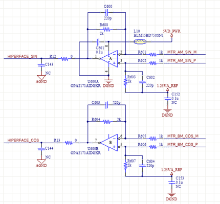
Customer is modifying the TIDA-00202's circuitry of the SINE and CONE Signal conditioning for hyperface requirement.

There are some R, C and OPA changed(Removed buffer, change gain value, filter, OPA..). Please find the schematic.

Customer prefers to use existing OPA of the OPA2171(BW:3MHz) instead of OPA2365(BW:50MHz) on the design. Is there any side-effect?  

Hiperface application on the communication rate is just 250KHz, they think OPA2171 would be good enough on Hyperface design. Is this correct?

Customer: WW class

Max. Motor Speed: 3000rpm/205KHz

Schematic based on TIDA-00202

Customer Schematic.

  • Hello Brian,

    we will look into this. We need to compare other parameters of the op amp like offset/drift, noise, slew rate, etc. too.

    We will do a TINA spice simulation to see if not only the bandwidth but especially other parameters like offset and offset drift, noise, etc.
    have an impact. I assume with 250kHz you refer to the maximum frequency of the analog Sin/Cos output?

    I expect results during next week.

    Regards,
    Martin
  • Thanks Martin.

    The electrical requirements are 0.6-1.2Vpp, 250KHz and 11bit resolution for hyperface application.

  • Hello Brian,


    The circuit shown above does not have any additional passives for termination and as such is not compliant to HIPERFACE suggestion from Stegman, which we considered in TIDA-00202. HIPEFACE recommend 130-ohm termination, 1k PDs, and  10k input impedance w/ the op amp for differential to single-ended conversion. To meet that recommendation, increase the input resistor to 10k (from 1k) and add the passive front end per TIDA-00202, as shown below prior to the amplifier. NOTE: R56, R92 can be removed, C70, C74, C76 were added for test and debug and are not part of the HIPEFACE spec, as well as the Schottky clamping diodes. These were added for better EMC immunity.


    Regarding OPA171 versus OPA365. We will provide a TINA model of the TIDA-00202 analog circuit within the next 2 month on the TIDA-00202 design folder on TI.com. Then any customer can simulate other op amps versus the OPA365.

    This should enable the customer to simulate with other TI op amps than OPA365 and take their own conclusion from the simulation results.

    Below I’ve listed some key parameters for considering OPA171 vs. OPA365.


    Slew rate

    • The OPA171 typical slew rate of 1.5V/us is slightly higher than the maximum slew rate for a circuit with a DC gain of 2 and a -3dB cut-off frequency of 250kHz up to 250kHz with inputs signals up to 1.2Vpp. See table below.  

    Input voltage
    [Vpp]

    Input Frequency
    [kHz]

    Gain (DC)

    Gain @Frequency (-3dB)

    Output Voltage @Frequency
    [Vpp]

    Min. Slew Rate [V/us]

    OPA365

    OPA171

    1.2

    150

    1.65

    1.155

    1.386

    0.653137113

    25V/us

    1.5V/µs

    1.2

    150

    2

    1.4

    1.68

    0.791681349

    25V/us

    1.5V/µs

    1.2

    250

    2

    1.4

    1.68

    1.319468915

    25V/us

    1.5V/µs


    Offset & Offset Drift

    • The initial offset of the OPA171 is 250uV, while the OPA365 is 100uV. With respect to 1Vpp, the offset error is 0.1% with OPA365 (1 LSB at 10-bit) and 0.25% (2.5 LSB at 10-bit).  If the initial offset can be calibrated by the customer, the higher offset of OPA171 might not be an issue.

    • The offset drift of the OPA171 (0.3V/us) is lower than the OPA365 (1V/us), hence the impact of the offset drift on the accuracy should be lower than w/ OPA365 used in TIDA-00202.


    Noise

    • With regards to 11-bit resolution (equivalent to 0.05%) the total input voltage noise at 1Vpp input signal should be below 500uV. The noise with both op amps should be below that threshold: The input voltage noise (0.1-10Hz) is 5uVpp (OPA365) and 3uVpp (OPA171). The input voltage noise density of the OPA171 is 14nV/sqrt(Hz) at 1kHz, while the OPA365 is 4.5uV/srqt(Hz) at 100kHz. At 250kHz bandwidth the voltage noise equals around 7uV (OPA171) and 2.2uV (OPA365).

    Common mode voltage range

    • The OPA365 is a rail-to-rain input op amp, while the OPA171 is rail-to-rail output only. With a 5V single supply the maximum input common mode voltage is 3V with OPA171, while 5.1V with OPA365.
      For HIPERFACE encoders with 2.5V DC common mode voltage the input common mode voltage with the circuit given below (OPA171, G=2, Bias=1.25V) is 2.083V. If additional common mode is added due to noise coupling,
      of course the OPA365 offers a 2V higher margin.

    Regards,

    Martin