This thread has been locked.

If you have a related question, please click the "Ask a related question" button in the top right corner. The newly created question will be automatically linked to this question.

DRV135: Audio line driver DRV135UA

Part Number: DRV135
Other Parts Discussed in Thread: TLE2426

Hi ,

I would like to know some parameters of DRV135UA, see below questions:

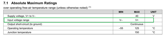
1. The minimum single power supply of V+ (Pin 6 ) and V-(Pin 5) connect to GND? 

2. Does single Power of V+ (V-(Pin 5) connect to GND) can support 5V or 14V ? 

3. Does Vin need to have a DC bias ? What's the DC bias level of Vin needed ?  Can it be a half divided of V+

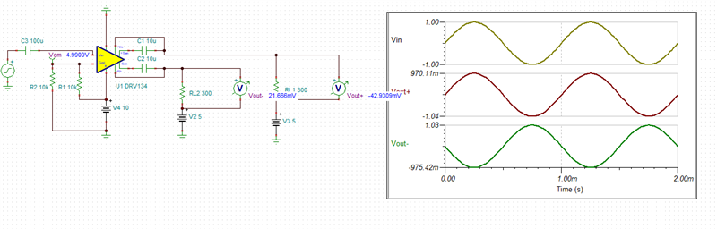
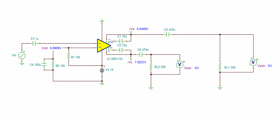
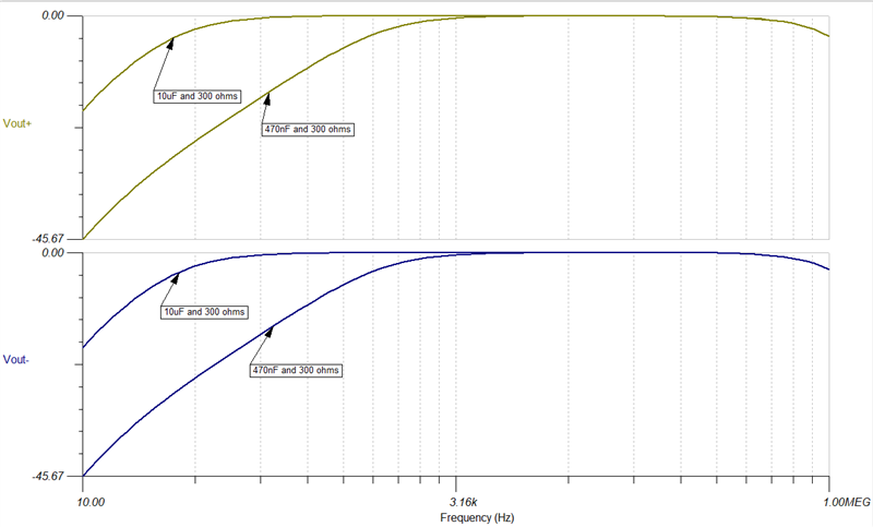
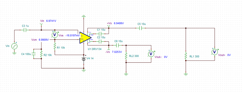
    See attached schematic as well.

Thanks!

TT_Chin

DRV135UA.pdf

  • Hello,

    We only recommend operating this device with split supply configuration with the GND pin at 0V potential. 

  • Hi Chris,

    Thank you for your answer.

    I saw you have suggestion a solution of single power supply connection of DRV135UA in E2E one month ago.

    In the schematic, you connected 10V on V+ and  GND(0V) on V-, divide half voltage of V+ by two 10K ohm resistors and connect it  to GND pin of DRV135UA. (see the picture below I copied from your message before)

    According to your schematic ,can I change V+ from 10V to 14V ? Please help to check the schematic as attached.

    Thank you for your help!

    Sincerely,

    TChin

    DRV135UA_1.pdf

  • Tchin,

    Thank you for pointing this out. I have discussed with a colleague and we have determined that single supply operation is ok. The minimum specified supply is +/-4.5V which would translate to 9V on a single supply and the max is +/-18V which translates to 36V single sided. 

  • Hi Chris,

    Thanks for updated about DRV135 can support single power.

    I would like to double confirm if following connections are a right connection of single power. Or you can see attached, help to check if the circuit is a right connection of single power ? any concern about the circuit ?   Thank you for your help!

    Pin 6(V+): connect to 14V

    Pin 5(V-): connect to 0V (ground level)

    Pin3 (GND): Half of V+.(divide by two resistors)

    Sincerely,

    Tchin

    DRV135UA_2.pdf

  • Tchin,

    This looks correct. Operating at 14V is sufficient and you are providing a level shift of 7V ( mid supply) on the GND pin. Just make sure your output load is also referenced to mid supply as well as shown in my simulation. 

  • Hi Chris,

    Thank you for your answer.

    I saw there are two voltage indications of 21.666mV and -42.9309mV in your simulation. What do the voltage mean ?

    By the way, Is the value 300 ohm of RL1 and RL2  just a reference , not relevant to any circuit ?

    If we have a DC block capacitor between +Vo/-Vo of DRV135 and Line_in_P/N of Audio code, does DRV135 still need output load reference to middle supply ?  Also See attached for more detail of our circuit.

    Thank you for your help!

    Sincerely,

    Tchin

    DRV135UA_3.pdf

  • Hi Chris,

    Any feedback about my questions ?

    Thank you for your help!

    Sincerely,

    TChin

  • Hell Chris,

    Any feedback for the discussion?

    Sincerely,

    Tchin

  • Hello TT,

    Chris is on holiday this week. I don't work with the DRV135 often, but will try to assist until he returns I believe this coming week.

    I looked over your schematic and adding the DC blocking capacitors at the DRV135 outputs should remove the need for the output loads to be connected to mid supply. 

    Looking over the rest of the circuit I am a little concerned about the impedance that pin 3, GND pin sees looking back into the 10 kilohm resistive divider. It amounts to 5 kilohm, which is quite high. I suggest bypassing the resistive divider with a capacitve divider i.e. consider putting a 10 uF or higher capacitor across each 10 kilohm resistor. That will reduce the impedance significantly and should help preserve the DRV135 performance. Alternately, use a supply splitter such as the TLE2426, with bypass capacitors from each supply to its output.

    https://www.ti.com/lit/ds/slos098d/slos098d.pdf

    If you can wait until Chris returns early next week I think it would be good to have his opinions on your application because he has the most current knowledge about the DRV135.

    Regards, Thomas

    Precision Amplifier Applications Engineering

  • Hi Thomas,

    Okay, I can wait until Chris returns this week.

    Thank you for your help!

    Sincerely,

    Tchin

  • Tchin,

    The reason the outputs have 21.6mV and -42.955mV is due to not having DC blocking caps on the outputs. If they are added then the load does not need to be referenced to mid supply. Below you can see that the Vout- and Vout+ values are now 0V. The 7V of common mode is seen at the ground pin to level shift in order to accommodate the single supply operation. In addition I added a filter cap across R2 = 10k in order to filter out any supply noise seen at this node. Alternatively, the supply splitter that Tom suggested is a good option as well. The 300 ohm load resistors are just a reference example. 

  • Tchin,

    I also wanted to follow up on the frequency response. My last post showed the 470nF and 300 ohm load. These two components will impact the frequency response. See below. 

  • Hi Chris,

    Okay, Thank you for your great support!

    By the way, can you share which simulation tool you used in above circuit ? 

    Sincerely,

    Tchin

  • Tchin,

    Glad to be of help! The tool I used is our free Spice simulator Tina Ti. 

    https://www.ti.com/tool/TINA-TI

    It would help me a lot if any of my answers that helped were marked as resolved. Feel free to reach out with any further questions.

  • Hi Chris,

    Okay, thank you!

    Sincerely,

    Tchin

  • Hi Chris,

    I have one more item need discuss with you. 

    The circuit you simulated above, there is a DC block capacitor (C3) in front of  Vin of DRV135UA. So the DC offset is 0 volt on Vin of DRV135UA.

    But if DC offset is 0 volt, the minimum swing voltage less than 0 volt. See the following waveform you post before.We can see the minimum voltage is -1 volt. 

    Datasheet define the voltage range of Vin is between V+ and V-, according to the schematic, V- connect to GND (0 volt), it means the minimum voltage (-1V) is out of V- (0 ). Do you have any concern about this ?

    Sincerely,

    Tchin

  • Tchin,

    The common mode is shifted on the gnd terminal so in turn the input terminal has the same voltage (Vcm) at it's terminal minus the Vos of the device. As seen below the inputs are 16.82mV apart. 

    This is achieved internally as seen in the simplified schematic below. If the common mode voltage of the non-inverting terminal of A1 is 7V then the inverting terminal is also close to 7V. 

  • Hi Chris,

    Okay, Thank you for your answer.

    Sincerely,

    TChin