This thread has been locked.

If you have a related question, please click the "Ask a related question" button in the top right corner. The newly created question will be automatically linked to this question.

OPA1671: maximum voltage of the non-inverting input

Part Number: OPA1671

Hello Guys,

Good day.

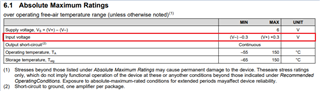
Our customer wanted to know what is the maximum voltage the non-inverting input of this part can withstand without being powered?  He's using this opamp for a buffering circuit in his design to measure battery voltage.  So the non-inverting input could see 0-1.6v DC before the opamp is powered up by the system.

Thanks and regards,

Art

  • Hi  Art,

    In OPA1671, I believe that that input voltage can only be approx. 0.3V above V+ supply, which is zero. 

    What is the application? OPA1671 is audio amplifier. If this is battery application, I would recommend OPA2206 , which it has input overvoltage protection up to 40V, even it is unpowered. 

    Best,

    Raymond

  • Hi Art,

    We don't characterize our PRAMPS op amps with unusual supply and input conditions. There are just too many possibilities to make it practical so we keep it to the normal, expected supply conditions. 

    Let me add a little to the information Raymond provided regarding the OPA1671. When you mention the OPA1671 is "without being powered" can we make the assumption that its V+ and/or V- pin(s) are seeing a high impedance circuit condition? As Raymond pointed out the OPA1671 input voltage range from table 6.1 Absolute Maximum Ratings as (V-) - 0.3 V to (V+) + 0.3 V and that is when powered normally. The range tells us the OPA1671 has ESD protection diodes from each input to both the V+ and V- pins internally. The "0.3 V" excess beyond the supply rails is below 0.6 V and that maximum assures the ESD diodes stay off.

    If the OPA1671 supply pins are floating in a high impedance OFF state, and a positive +1.6 V voltage is applied to the non-inverting input, current can flow to the V+ supply pin via an ESD diode. The diode is forward biased and it will provide the usual 0.6 to 0.7 V voltage drop so only about +1 V appears at the V+ pin. Some current may flow through the op amp through various paths, but the +1 V V+ it isn't going to be much since the minimum supply voltage is +1.7 V. The OPA1671 has CMOS FET inputs and I don't expect there will be a latch condition created which can be a concern for some op amp designs.

    Since TI doesn't make any assurances about what the OPA1671 will do when an input voltage is applied before the supplies are present the user assumes the risk. However, based on the information provided the risk to the OPA1671 appears low. 

    For a discussion on a subject very close to this scenario see An Engineer’s Guide to Designing with Precision Amplifiers, "The mystery of the depleted coin cell" on Page 30.

    https://www.ti.com/lit/eb/slyy209/slyy209.pdf

    Regards, Thomas

    Precision Amplifiers Applications Engineering