This thread has been locked.

If you have a related question, please click the "Ask a related question" button in the top right corner. The newly created question will be automatically linked to this question.

OPA1637: opa1637

Part Number: OPA1637
Other Parts Discussed in Thread: PGA2500, , THP210, PGA2505, OPA1632

Hi, I am trying to buffer the pga2500 to an ADC with OPA1637

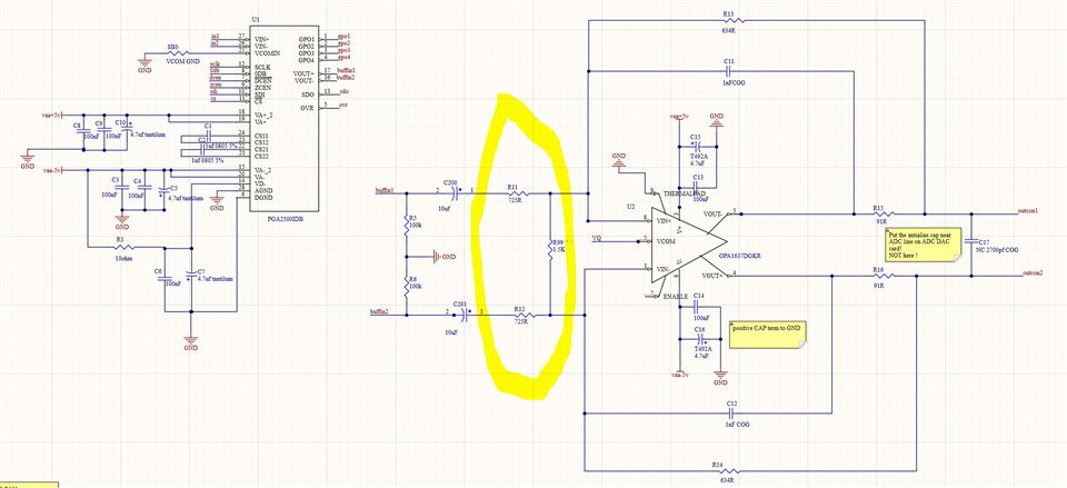
I want the pga2500 to be buffered with an op amp that is setup with low pass neg feedback filter > 1mhz

I am only using +/-5v rails for PGA2500 and would like to use the same power rails for the opamp.

the PGA2500 vcom connected to 0v ( GND ) for maximum SNR. ( I am NOT connecting PGA2500 VCOM to ADC 2.5v )

there are DC filter caps between the PGA2500 and OPA1637.

OPA 1637 is biased by VCOM supplied by the ADC ( buffered by OPA143 )

I am using an simple passive /2 U attenuation resistor network ringed in yellow from pga2500 8.2Vpp max swing down to less than 4Vpp for the

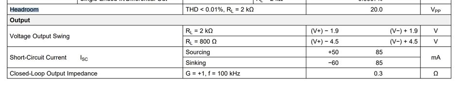
OPA1637 inputs. So this should be ok for +/-5v power headroom ?

I am still getting some pops and audio dropouts on high inputs.

When I hook up the AC coupled scope to the OPA1637 inputs ( either side of the R99 in the U attenuation )  I notice the phase of the audio is the same although the outputs of

the PGA2500 are inverse.

I have been recommended part THP210 instead of OPA1637 , but would like to know what causes the inverted phase at input and what causes the audio 

dropouts ? the inputs OPA1637 inputs have DC filter caps so no DC from VCOM bias at PGA2500 outputs. 

I think THP210 has same pins so I can try and drop in onto the prototype board but would like to know what is going wrong with OPA1637 1st ! 

Any ideas would be much appreciated !


  • I changed R11 R12 R13 R14 to 2K as in opa1637 datasheet examples and changed the bridge resistor to 4.3K

    I still get dropouts on load audio input although things have improved with these resistor values.

    I also removed R5 R6 to make sure they were not overloading the PGA2500 output impedance.

    I can probably make the filter work with the 2k resistors.

    Is +/- 5v pwr on OPA1637 enough for this application ?

  • Ben,

    We are currently looking into this. I will respond tomorrow.

  • great thanks for letting me know Chris.

    I just discovered this in PGA2505 datasheet ( same PGA as PGA2500 but with less gain steps ).

    In this diagram there is no attenuation before OPA1632 and with the 2.5v bias from the ADC connected to the OPA1632.

    It doesn't really explain if the PGA VCOM is also connected to the bias as the OPA1632 inputs would also be biased to 2.5V. I think there

    should be DC filter caps or VCOM connected to bias in that diagram.

    I guess the 1K and 470ohm are working as dividers so no need to attenuate before input of the buffer. 

    I have some OPA1632 so I can try this but datasheet says you 1.9v on rails headroom so I suppose its a max swing of +/-3.1Vpp

    I went with the OPA1637 hoping to get nearer 4.1Vpp swing at the ADC.

  • Hi Biles, 

    • If the expected PGA2500 output signal is ±8.1Vpp differential, the PGA2500 VCOM pin could be connected to GND to allow headroom for the PGA2500 output swing.  
    • The OPA1637 (or THP210) can accommodate an input differential signal of ±8.1Vpp with 0V common-mode when setup in an attenuator configuration to produce an output differential signal of ±4.096Vpp while powered by bipolar ±5V supplies. The OPA1637 VCOM pin voltage needs to be biased according to the input common-mode specification of the ADC.  (Some differential input ADCs require a strict fixed common-mode of VREF/2 where VREF is the ADC voltage reference while other ADCs have a a flexible input common-mode specification).  What ADC device is used in this application?  I set VCOM = 2.5V per your circuit above.
    • Yes, the most common way to attenuate signals when using a fully differential amplifier (FDA) is to set the gain by the ratio of the feedback and input resistors. There are many possible attenuator/filter circuit topologies that can be used for this purpose. Below is a very simple attenuator example with input resistor of 2.1kΩ and 1.02kΩ setting the circuit to an attenuation (gain) of 0.486V/V.  The circuit accepts a ±8.1Vpp differential input signal from the PGA2500 and produces an output of approximately ±3.94Vpp.  This circuit using 1nF feedback capacitors is stable driving the 100Ω-1nF-100Ω (R-C-R) filter at the output of the FDA.  Attached is the TINA transient and open-loop stability analysis showing a phase margin greater than 45-degrees. If required, we can re-adjust the feedback and input resistor values to obtain the desired attenuation. Please let me know if you require a different attenuation.
    • Another attenuator circuit example for the OPA1637 (or THP210) is shown on the THP210 datasheet on Figure 9-16, page 31 implementing a low-pass, second order, Butterworth filter. This circuit will need to be modified per the required attenuation, frequency response and re-verified for stability after the modification with simulation.

    Below is a simple/basic attenuator circuit (and TINA simulation file) using the OPA1637/  Please let me know if you have questions,

    Thank you and Regards,

    Luis Chioye

    TINA simulation files:

    OPA1637_attenuator1_TINA.zip

  • Hi Luis,

    I am using ADC Cirrus Logic CS5368 and I am getting 2.65V VQ ( VCOM ) from the device and the full-scale Differential Input Voltage should be 1.13*VA. VA is 5V.

    I think I need Circuit Attenuation set to 0.68V/V    ADC 5.65v  /  PGA 8.1v   = 0.697 gain

    I took away the bridge resistor and did something like your circuit with RG of 4.3K and RF at 2K.

    any reason you chose 1.02k for RF1 & RF2 and not 2K as in datasheet ? guess that's just to do with the filter you made.

    I'll try and figure out the 0.68V/V using TINA now. Much appreciated if you want to have go :)

    I think it should be something like  RG 3k RF 2K ( or RG 1.5K RF 1.01K in your circuit ) ?

    One question , does the 2.65V on the Vocm pin raise the input pins of the OPA1637 to 2.65V ?  in other words do I need to keep the DC blocking caps from PGA2500 with PGA VCOM connected to GND? 

    I was trying to use PSPICE for TI with the OPA1637 spice model but the AC analysis graph was getting stuck and giving me trouble. I guess TINA is more reliable ? 

    thanks for your help on this !

  • Hi Biles,

    If you require a full-scale range at the ADC input with amplitude of ±5.65Vpp, with VOCM set at +2.65V, the out+ and out- pins of the OPA1637 will need to swing to approximately 2.65V + 5.65V/2 = +5.475V and 2.65V - 5.65V/2 = -0.175V.  The V+ positive supply for the OPA1637 will need to be increased to V+ ≥+6V per the AOL spec, to keep the OPA1637 outputs inside the linear region.  Note: the output can swing to about ~270mV from the rails depending the load and temperature conditions per the output swing specifications, but it is best practice to use the most conservative AOL open-loop gain output swing condition from the rail, ensuring the amplifier stays well within the linear region with plenty of margin providing the best performance over frequency.

    There is flexibility on the resistors that can be used for the FDA input and feedback. There are some trade-offs between power, noise, loading of the amplifier, etc.   

    Using the larger resistor values will increase the thermal noise contribution of the resistors, and increase the noise due to the input current noise of the amplifier interacting with the resistors. Nevertheless, the increase in the resistor values will also result in lower current consumption.  Smaller resistor values will result in lower noise, with a trade-off in the increase of current consumption.  Another factor to consider when scaling the feedback and input resistors of the FDA, is the input impedance of the FDA.  The input impedance is determined by the value of the input resistors, and therefore the designer needs to consider the drive capability of the preceding circuit or sensor driving the FDA when scaling the resistor values.  The THP210 offers the super-beta input bipolar transistors, that provide a reduction on input bias current, and a reduction of the amplifier input bias current noise. This lower bias current provides a reduction on the initial DC and drift errors in the circuit, and allow the use of larger resistor values with a relative smaller impact to noise, offset and drift errors.  The datasheet tends to recommend 2kΩ feedback resistors, since this is a good performance compromise between noise, DC errors and power consumption.  However, if current consumption is not a major concern in your application, the THP210 is flexible and you can certainly choose to use 1-kΩ feedback resistor, providing a reduction in the noise.  For example, the datasheet tested circuit of figure 9-12 on section 9.2.2 uses 1kΩ feedback resistors and produces low noise and low distortion as shown in the FFT results.  In general, I tend to avoid using resistor values that produce a circuit overall effective load much smaller than 1-kOhm as they may start to load the fully-differential amplifier resulting in an increase in harmonic distortion. 

    For example, using RIN=3.01kΩ and RF=2kΩ with differential R-C-R filter of 100Ω +1nF+100Ω, and CF=510pF feedback capacitors offers a total output noise of ~6.88-µVRMS with a bandwidth of ~147kHz (you can change the bandwidth by adjusting the feedback capacitors per your requirement).  The load circuit seen by the OPA1637 is about ~5.01kOhm (plus the impedance of the R-C-R filter over input frequency) at each output so this is probably perfectly fine.  At this particular bandwidth, reducing the resistors to RIN=1.5kΩ and RFB=1kΩ appears to make a very small or negligible effect in noise.   The PGA2500 can easily drive the input impedance of the FDA with the proposed resistors on both the circuits discussed above; and you can always simulate the noise, adjust bandwidth, and resistor values in TINA and decide what is the best trade-off per your requirement. I think the RIN=3.01kΩ and RF=2kΩ is optimal.

    You can also check this post, it discusses this resistor selection topic in more detail, with reference to articles:

    https://e2e.ti.com/support/amplifiers-group/amplifiers/f/amplifiers-forum/991784/thp210-thp210-gain-setting-regarding?tisearch=e2e-sitesearch&keymatch=thp210#

    The voltage right at the input terminals at the VIN+, VIN- of the OPA1637, is a function of the voltage at the other side of the input resistor and the voltage at the output of the OPA1637. Yes, as you set the VOCM to 2.65V, this will raise the output common-mode slightly, but since the PGA2500 output is at 0V common mode you are well within the common-mode range. Essentially the voltage at the input terminal, is the voltage divider that forms between the RG/RFB resistors.  The VICM refers to the input common-mode voltage right at the input terminals of the OPA1637 Fully-Differential amplifier.  The specification on page 6 of the OPA1637 datasheet defines the VICM valid range as (V_VS-) + 1V <VICM < (V_VS+) - 1V; where this is the input common-mode voltage right at the input terminals of the OPA1637 need to be at least 1-V from both supply rails.  Keeping the PGA2500 VOCM = 0V and OPA1637 VOCM = +2.65V will keep the input terminals well within inside range when powered with +6V and -5V.  Strictly speaking, from the input common-mode perspective, it is not necessary to add the DC blocking capacitors in this case.  However, if you wish to add the DC blocking capacitors at the inputs of the amplifier to cancel a DC offset coming from the signal chain prior the OPA1637, you can certainly do so. 

    Below is an example transient simulation with the RIN=3.01kΩ and RF=2kΩ with differential R-C-R filter of 100Ω +1nF+100Ω, and CF=510pF, V-=-5V and V+=+6V, VOCM=+2.65V that you can adjust / modify per your application requirement.  

    Thank you and Regards,

    Luis Chioye

    TINA File:

    OPA1637_transient_attenuator3.TSC

  • Hi Luis , I was trying to avoid using a higher voltage rail since I am switching 8 individual preamp cards on/off as a power saving feature. adding the extra power rail drastically complicates the power switching on the 8 cards. I am switching the +/-5v with optomos for isolation from digi. 

    I do however have +/-10v in the design for line driver and HP driver cards

    I just noticed the Power Down PD pin on the OPA1637 ,  I think I can switch the PD pin with +5v PGA2500 rail ( on / off ) driving an N-type MOSFET , so when the +/-5v rails are switched off the OPA1637 goes into low power mode.

    That way I can leave the OPA1637 +10V connected when the card is switched off and the power loss would be around 2uA

    can you sergest a TI N-type mosfet that might work in this scenario?

    Other than that I would have to change ADC to reduce that VCOM and even then there isn't much headroom on the +5v rail ! 

    Thanks for your explanation of your resistor choice :) I will check out the link you posted.

  • HI Biles,

    Let me look into a NMOS diode for this application, and get back to you shortly.  

    Also, if you are planning to leave the +10V supply connected to the OPA1637 and place the device in shutdown mode, please keep in mind that the device will always require a connection to a negative supply to ensure proper current flow through the device.  In other words, the negative supply pin must not be left open or floating, and must be set to a voltage below all the other pins of the device, to ensure proper current path and avoid damage.

    Below is a useful TI Precision Lab session that discusses this topic.

    https://training.ti.com/ti-precision-labs-op-amps-electrical-overstress-introduction?context=1139747-1139745-14685-1138807-13956

    Thank you and Regards,

    Luis 

  • Ah, ok, maybe it's better to just route +/-5v and +/-10V into the cards then.

    The PD mode only saves approx 16mA across 8 channels anyway. opa1637 is very low power.

    Update: 

    I changed RG & RF to 3K & 2K and  cut off the +/-5V to OPA1637 and injected +/-10V on my prototype card.

    There is no dropout now on load inputs and it the audio is incredibly clean.

    I think I will just run +/-10v rails to the buffer op amps and leave them switched on. 

    The PGA2500's use much more power so I will keep the switching on those.

    Thanks for your help.

    Ben

  • Hi Ben,

    That's great news. Thank you for the update.

    Another suggestion for the PGA2500, since you will be switching supplies on/off, a recommendation is to add TVS or zener protection diodes on the PGA2500 ±VA supplies to ensure all pins stay within the absolute maximum ratings, and no abnormal conditions occur during the power up and power down sequence.  For example, during the power-up sequence, if the negative supply is off, diode D6 will be forward biased, provide a path of current between the positive and negative supply, preventing the abnormal current flow.,. Once the negative supply powers on, diode D6 will be reverse biased, and the device powers up normally.

    Thank you and Best Regards,

    Luis

  • I will do this in case one side of the supply goes bad.

    I do monitor the power supply voltages with an ADC on the MC so the opto's can shut off the PGA's

    but this seams like a better fail safe.

    I'm assuming the TVS have to be rated for maximum possible current of the supply ?

    I designed an ultra low noise +/-5v supply that can deliver around +/-850mA , would 1A scotchy rated at around 12V work ? 

    Any common TI TVS I can use for this you know of ? 

  • HI Biles,

    Choose a uni-directional TVS diode with a current rating of ~1A in this case. Select a Zener / TVS diode with a reverse standoff voltage or reverse working maximum voltage of 5V, a breakdown voltage at 5V or slightly above 5V, and a low clamping voltage as close as possible to the absolute max rating of the device. Although the clamping voltage of the diode may exceed the max ratings of the device, the protection diode will still offer a level of protection.  There are discrete TVS diodes available in the market from manufacturers such as Bourns, Littlelfuse and Diodes Inc, etc. that could work well in this case.  You could also post a question on the Interface forum where an expert on the TI ESD protection devices may provide a suggestion. 

    In this case, the uni-directional TVS diode on the negative supply will help provide a current path for the current during the power-up sequence in the event where the positive supply connects or ramps up before the negative supply or during a fault condition, and the diode will forward bias and keep the negative supply close to GND, in the case the negative supply is high impedance or disconnected.

    Thank you and Regards,

    Luis