


Hello,
We have seen strange THD+N characteristics at Vdd=3.3V RL=33ohm SE input configuration on own PCB, not EVM.
There is two peaks before Voltage clipping as attached image, we also observed switching noise at positive signal peak.
(Horizontal output power of AP graph is not calibrated)
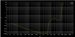
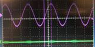
At no load condition this noise is disappeared. It seems charge pump noise related phenomena but it positive side.
Could you give us check point of PCB layout or another critical GND connection etc.
Regards,
Mochizuki
