Dear Sirs,
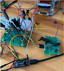
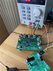
I am using the DRV594 Evaluation kit to test the possibility of driving a Peltier Module (2.7Ohms resistance). DRV594 is supplied with 3.3V and driven the following way:
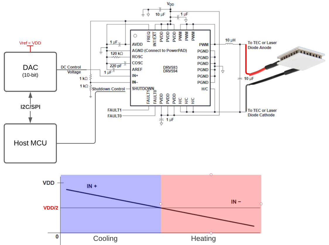
VIN- is kept to VDD/2 and VIN+ is set by the output of the 10-bit DAC module (controlled by the host MCU). According to the formulas given in DRV594 datasheet:
Vload = D x VDD;

D = A (Vin+ - Vin-) / VDD;

A = 14.5V/V in the case of DRV594
A = 2.3V/V in the case of DRV593
The difference of about 200mV between VIN+ and VIN- inputs should lead to a 100% duty cycle, i.e. Vload = VDD.
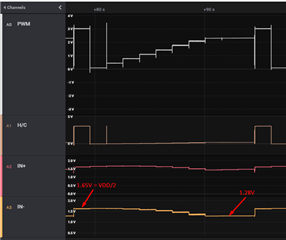
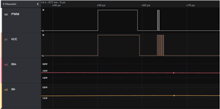
By using a logic analyzer, I can confirm that the VIN+/VIN- inputs of the DRV594 are driven properly (at some point, there is a difference of ~200mV between VIN+ and VIN-):

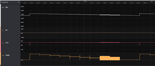
However, the output pins of DRV594 (PWM and H/C) remain at 0% duty cycle):
Do you have any idea about what I am doing wrong here?
Thanks in advance for your time and efforts. Looking forward to hearing from you.
Sincerely,
Bojan.


