This thread has been locked.

If you have a related question, please click the "Ask a related question" button in the top right corner. The newly created question will be automatically linked to this question.

TLV320DAC3100: I2C communication failure after configuring

Part Number: TLV320DAC3100

Hello,

I am having I2C communication issues after configuring the DAC3100 on a custom board where it periodically NAK's reads and writes and never recovers. I ported my driver directly from a previous custom board hardware revision that has been working for years. I am puzzled as to why the driver exhibits I2C communications errors on the new hardware.

Old hardware details (Working):
DAC: DAC3100 TI 9AI AKH2 G4    *
AVDD: 2.8V
SPKVDD: 2.8V   *
IOVDD: 2.8V
DVDD: 1.8V
I2C Pull-up: 1.5K Ohm   *
New hardware details (I2C errors - NAK):
DAC: DAC3100 TI 131 C265 G4    *
AVDD: 2.8V
SPKVDD: VBAT (4.0 - 4.2V)  *
IOVDD: 2.8V
DVDD: 1.8V
I2C Pull-up: 2.2K Ohm    *
Note: Hardware differences are denoted with an asterisk *
Register configuration (Same on both old and new hardware):
/* an array of address/value pairs */
static const uint8_t aInitRegs[] = {
  0x00, 0x00,   // select page 0
  0x01, 0x01,   // software reset
  0xFE, 1,      // delay 1 ms (Parser implements via vTaskDelay())

  0x00, 3,      // page 3
  0x10, 0x01,   // use internal osc for delay timers
                 
  0x00, 0x00,   // select page 0
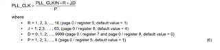
  0x04, 0x03,   // PLL_CLKIN=MCLK, CODEC_CLKIN=PLL_CLK
  0x05, 0x11,
  0x06, 40,     // set PLL for DAC_FS=8KHz: J=40, R=1, D=0, P=1
  0x05, 0x91,
  0xFE, 10,     // delay 10 ms (Parser implements via vTaskDelay())

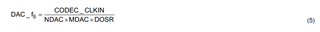
  0x0B, 0x81,   // NDAC=1
  0x0C, 0x90,   // MDAC=16
  0x0D, 0x02,   // DOSR=640
  0x0E, 0x80,
  
  0x1B, 0x00,   // mode I2S, wordlength 16, slave mode
  
  0x3C, 4,      // processing block 4

  0x00, 0x08,   // select page register 8
  0x01, 0x04,   // turn on adaptive filtering
  
  0x00, 0x01,   // analog blocks, select page register 1
  0x23, 0x40,   // LDAC routed to mixer/amp, RDAC not routed anywhere
  0x2A, 0x04,   // unmute class-D, 6 dB gain
  
  0x20, 0x86,   // power-up class-D
  0x26, 0x8C,   // left analog volume routed to class-D, vol = -6 dB
  
  0x00, 0x00,   // page 0
  0x3F, 0xB0,   // LDAC on, RDAC off, LDAC=(L+R)/2
  0x41, 0x30,   // LDAC gain 24 dB
  0x42, 0x81,   // RDAC gain -63 dB
  
  0x40, 0x00,   // unmute L,R channels
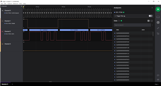
};
At this point, if I attempt to read back registers on the new hardware, I start getting driver errors due to NAK.
i2c=1,2,30,00,00
Test I2C write
I2C write - Slave Addr: 0x30, Register: 0x00, Payload: 0x00
> i2c=0,2,30,04,1
Test I2C read
I2C read - Slave Addr: 0x30, Register: 0x04, Number of bytes: 1
Received: 0x03
> i2c=0,2,30,05,1
Test I2C read
I2C read - Slave Addr: 0x30, Register: 0x05, Number of bytes: 1
Received: 0x91
> i2c=0,2,30,06,1
Test I2C read
I2C read - Slave Addr: 0x30, Register: 0x06, Number of bytes: 1
Received: 0x28
>
> i2c=0,2,30,FE,1
Test I2C read
I2C read - Slave Addr: 0x30, Register: 0xFE, Number of bytes: 1
I2C read failed
> i2c=0,2,30,0B,1
Test I2C read
I2C read - Slave Addr: 0x30, Register: 0x0B, Number of bytes: 1
I2C write failed
I2C read failed
Oddly, if I never configure the DAC3100 registers and attempt to read all the registers back, I have no I2C communication issues:
>
>
> i2c=1,2,30,00,00
Test I2C write
I2C write - Slave Addr: 0x30, Register: 0x00, Payload: 0x00
>
>
> i2c=0,2,30,04,1
Test I2C read
I2C read - Slave Addr: 0x30, Register: 0x04, Number of bytes: 1
Received: 0x00

> i2c=0,2,30,05,1
Test I2C read
I2C read - Slave Addr: 0x30, Register: 0x05, Number of bytes: 1
Received: 0x11
>
> i2c=0,2,30,06,1
Test I2C read
I2C read - Slave Addr: 0x30, Register: 0x06, Number of bytes: 1
Received: 0x04
>
> i2c=0,2,30,FE,1
Test I2C read
I2C read - Slave Addr: 0x30, Register: 0xFE, Number of bytes: 1
Received: 0x00
>
> i2c=0,2,30,0B,1
Test I2C read
I2C read - Slave Addr: 0x30, Register: 0x0B, Number of bytes: 1
Received: 0x01
>
> i2c=0,2,30,0C,1
Test I2C read
I2C read - Slave Addr: 0x30, Register: 0x0C, Number of bytes: 1
Received: 0x01
>
> i2c=0,2,30,0D,1
Test I2C read
I2C read - Slave Addr: 0x30, Register: 0x0D, Number of bytes: 1
Received: 0x00
>
> i2c=0,2,30,0E,1
Test I2C read
I2C read - Slave Addr: 0x30, Register: 0x0E, Number of bytes: 1
Received: 0x80
>
> i2c=0,2,30,1B,1
Test I2C read
I2C read - Slave Addr: 0x30, Register: 0x1B, Number of bytes: 1
Received: 0x00
>
> i2c=0,2,30,3C,1
Test I2C read
I2C read - Slave Addr: 0x30, Register: 0x3C, Number of bytes: 1
Received: 0x01
>
> i2c=1,2,30,00,08
Test I2C write
I2C write - Slave Addr: 0x30, Register: 0x00, Payload: 0x08
>
> i2c=0,2,30,01,1
Test I2C read
I2C read - Slave Addr: 0x30, Register: 0x01, Number of bytes: 1
Received: 0x00
>
> i2c=1,2,30,00,01
Test I2C write
I2C write - Slave Addr: 0x30, Register: 0x00, Payload: 0x01
>
> i2c=0,2,30,23,1
Test I2C read
I2C read - Slave Addr: 0x30, Register: 0x23, Number of bytes: 1
Received: 0x00
>
> i2c=0,2,30,2A,1
Test I2C read
I2C read - Slave Addr: 0x30, Register: 0x2A, Number of bytes: 1
Received: 0x00
>
> i2c=0,2,30,20,1
Test I2C read
I2C read - Slave Addr: 0x30, Register: 0x20, Number of bytes: 1
Received: 0x06
>
> i2c=0,2,30,26,1
Test I2C read
I2C read - Slave Addr: 0x30, Register: 0x26, Number of bytes: 1
Received: 0x7F
>
> i2c=1,2,30,00,00
Test I2C write
I2C write - Slave Addr: 0x30, Register: 0x00, Payload: 0x00
>
> i2c=0,2,30,3F,1
Test I2C read
I2C read - Slave Addr: 0x30, Register: 0x3F, Number of bytes: 1
Received: 0x14
>
> i2c=0,2,30,41,1
Test I2C read
I2C read - Slave Addr: 0x30, Register: 0x41, Number of bytes: 1
Received: 0x00
>
> i2c=0,2,30,42,1
Test I2C read
I2C read - Slave Addr: 0x30, Register: 0x42, Number of bytes: 1
Received: 0x00
>
> i2c=0,2,30,40,1
Test I2C read
I2C read - Slave Addr: 0x30, Register: 0x40, Number of bytes: 1
Received: 0x0C
>
Questions:
1. Does the change in SPKVDD need to be accounted for in the register settings?
2. Any idea what could be causing the DAC3100 to NAK I2C communication after being configured?
Thanks,
Derek
  • Hi Derek,

    First I would try to isolate SPKVDD change, one thing you can try is to initialize the device but without powering up the Class-D, ie. comment this line from your code:

      0x20, 0x86,   // power-up class-D

    If you're able to communicate through I2C by doing this, we could relate it to the speaker driver.

    Additionally, you can read back flag registers (register 44 to 46 on page 0) before and after initialization. Would help to check if device is detecting any issue by itself.

    Best regards,
    -Ivan Salazar
    Applications Engineer

  • Hey Ivan,

    Thanks for your reply. I read this after finding what I believe to be the issue. I noticed "rounded" edges on my I2C SCL and SDA signals and reduced the I2C clock from 400 KHz to 100 Khz and this mitigated my I2C issue. I no longer receive NAK's from the DAC3100 and can read all registers after configuring including enabling the class D amplifier. This leads me to believe a stronger pull-up is needed or I2C peripheral timing needs to be adjusted (DAC3100 is interfaced with a STM32L4 MCU). Strange how this would only be an issue after DAC3100 configuration.

    I have a new issue now. The speaker audio output is essentially a few squeaks and is unrecognizable. Ie, it is noise. I have compared the clocks between the old hardware and new hardware and compared I2S data and they are the same.

    Old Hardware (Working) New Hardware (Not working)
    WCLK 42.5 KHz 42.62 KHz
    BCLK 1.36MHz 1.36 MHz
    MCLK 10.93 MHz 10.87 MHz
    DIN NA NA

    The slight difference in clock frequencies could potentially be attributed to crystal tolerances.

    For reference, here is a screenshot of my I2S data:

    It has the following configuration:

    Frame Length: 32 bits (16 bits per channel)

    Audio file (.wav): 44.1 KHz, Stereo, 16-bits per channel

    I also read the error bits from the device and both registers were 0x00.

    > i2c=1,2,30,00,00
    Test I2C write
    I2C write - Slave Addr: 0x30, Register: 0x00, Payload: 0x00
    >
    > i2c=0,2,30,2C,1
    Test I2C read
    I2C read - Slave Addr: 0x30, Register: 0x2C, Number of bytes: 1
    Received: 0x00
    >
    > i2c=0,2,30,2E,1
    Test I2C read
    I2C read - Slave Addr: 0x30, Register: 0x2E, Number of bytes: 1
    Received: 0x00
    

    Edit: I found another status register (Page 0, 0x27 - Overflow Flags)

    Value: 0xA0 -> bit 7 (Left channel overflow) and bit 5 (Barrel shifter output overflow)

    Questions:

    1. Do I need to change any DAC3100 register values to account for SPKVDD voltage change?

    2. Would the slight differences in I2S frequencies above cause unrecognizable audio or potential overflow?

    Thanks,

    Derek

  • Hi Derek,

    Thanks for the feedback on the I2C issue.

    Regarding your questions, let me add some comments:

    • There are no register changes required for different SPKVDD levels.
    • It could affect the playback. Actually I'm concerned about your described clocks. Data should be sampled at 44.1kHz but your actual clocks are lower than that for some margin at ~42,5kHz.
      • Is there any way to make the clocks closer to their expected values? ie 44.1kHz,1.4112MHz and 11.2896MHz?
      • How did you calculated your PLL values? It mentions DAC_FS = 8kHz. Although even by calculating DAC_FS using those values the DAC_FS is ~113kHz instead of 44.1kHz
      • You could try with the following clock settings:
        • PLL_P = 1
        • PLL_R = 2
        • PLL_J = 40
        • PLL_D = 0
        • NDAC = 4
        • MDAC = 4
        • DOSR = 128

    Best regards,
    -Ivan Salazar
    Applications Engineer

            Ratio     Ratio   Ratio    
      MCLK 10870000 10930000 11289600  
      BCLK 1360000 255.04458 1360000 257.176471 256 1411200  
      WCLK 42620 31.9099015 42500 32 32 44100  
       
    J 40  
    R 1  
    D 0  
    P 1 434800000 PLL_CLK 437200000 PLL_CLK 451584000 PLL_CLK
    N 1  
    M 6  
    OSR 640   113229.1667 DAC_FS   113854.167 DAC_FS     117600 DAC_FS
            Ratio     Ratio   Ratio    
      MCLK 10870000 10930000 11289600  
      BCLK 1360000 255.04458 1360000 257.176471 256 1411200  
      WCLK 42620 31.9099015 42500 32 32 44100  
       
    J 40  
    R 2  
    D 0  
    P 1 869600000 PLL_CLK 874400000 PLL_CLK 903168000 PLL_CLK
    N 4  
    M 4  
    OSR 128   424609.375 DAC_FS   426953.125 DAC_FS     441000 DAC_FS
  • Hey Ivan,

    I actually inherited this code and used it as is since it is working on previous hardware. It looks like the PLL constants are modified after initial configuration based on the played audio file frequency. For 44.1 KHz, the updated PLL settings are the following:

    44100, 
    { 
        0x00, 0x00,   // page 0
        0x05, 0x11,   // set PLL for DAC_FS=44.1KHz: J=8, R=1, D=0, P=1
        0x06, 840,     
        0x05, 0x92,   // power on PLL
        0xFE, 10,     // delay 10 ms
        0x0B, 0x84,   // NDAC=1
        0x0C, 0x94,   // MDAC=16
        0x0D, 0x00,   // DOSR=128
        0x0E, 0x80,
        0xFF
    }
    
    // "D" was previosuly configured as 0 (Zero)

    I tried your settings and have the same result in that the speaker squeals. Reading register 0x27 still returns a value of 0xA0 -> bit 7 (Left channel overflow) and bit 5 (Barrel shifter output overflow). I created an excel sheet to configure the PLL. After plugging in your recommended values, DAC_FS comes out to be 441 KHz instead of 44.1 KHz. This can be seen in your table above.

    To calculate PLL_CLK, I am using equation 6 on page 54 of the DAC3100 datasheet:

    Where:

    PLL_CLKIN = MCLK = 10870000 on the new hardware

    R = 1 , J = 8, D = 0, P = 1

    Plugging all this in gives the following:

    PLL_CLK = 10870000 * 8 / 1 = 86960000 or 86.96 MHz

    To calculate DAC_fs, I am using equation 5 on page 52 of the DAC3100 datasheet:

    Where:

    NDAC = 1 , MDAC = 16 , DOSR = 128

    CODEC_CLKIN = PLL_CLK = 86960000 or 86.96 MHz

    Plugging all this in gives the following:

    DAC_fs = 86960000 / (1 * 16 * 128) = 42460.9 or 42.4609 KHz which is really close to WCLK of 42.62 KHz.

    Regarding getting the clocks closer to the expected values of 44.1kHz,1.4112MHz and 11.2896MHz, I will investigate this. I am using a STM32L4 with a 16 MHz crystal with a flexible PLL so it may be possible. If not, I will have to use the DAC PLL accordingly. I have attached the excel file I am using to calculate PLL values.

    Questions

    1. Is the 441 KHz value an error in your table or am I missing something?

    2. How close does DAC_fs need to be to WCLK? Does this need to be exact?

    3. Does WCLK need to be 44.1 KHz, or can it be 42.62 KHz so long as the DAC3100 DAC_fs is also ~42.62 KHz?

    4. Does TI have an official calculator for determining PLL divider / multiplier values based on a given MCLK and sampling frequency? This would be a useful tool.

    Thanks,

    Derek

    7411.DAC_PLL_Calculator.xlsx

  • Hi Derek,

    1. I must have input something wrong in my PLL calculator, below is the updated table. Since MCLK/BCLK/WCLK have specific ratio PLL would not be needed.
    2. I'm actually more concerned about incorrect clock settings in terms of ratios, than actual resulting frequency. However there is no specification of how close DAC_FS should be to actual WCLK. As long we clocks are matching the ratios for each bit is should be OK
    3. As mentioned on point 2 above, it is more important that the ratio from MCLK to BCLK and WCLK is correct, so that each bit and word can be sampled correctly.
    4. There is https://www.ti.com/lit/zip/slar163 calculator, you can use TLV320AIC31xx for TLV320DAC3100, their clock structure is similar

    I would first try with the clock settings without PLL, if ratios are correct then sampling should be good without using PLL.

    However if clocks are not matching correctly, PLL may be helping and could be the reason to use it. Then you can try some configuration to use PLL for correction. The main concern in this case is to make PLL_CLKIN*PLL_R*PLL_J.D/PLL_P > 80MHz and PLL_J > 4

    Best regards,
    -Ivan Salazar
    Applications Engineer

            Ratio     Ratio   Ratio    
      MCLK 10870000 10930000 11289600  
      BCLK 1360000 255.0446 1360000 257.1765 256 1411200  
      WCLK 42620 31.9099 42500 32 32 44100  
       
    J 40  
    R 1  
    D 0  
    P 1 434800000 PLL_CLK 4.37E+08 PLL_CLK 4.52E+08 PLL_CLK
    N 1  
    M 6  
    OSR 640   113229.17 DAC_FS   113854.2 DAC_FS     117600 DAC_FS
            Ratio     Ratio   Ratio    
      MCLK 10870000 10930000 11289600  
      BCLK 1360000 255.0446 1360000 257.1765 256 1411200  
      WCLK 42620 31.9099 42500 32 32 44100  
       
    J 1  
    R 1  
    D 0  
    P 1 10870000 PLL_CLK 10930000 PLL_CLK 11289600 PLL_CLK
    N 1  
    M 2  
    OSR 128   42460.938 DAC_FS   42695.31 DAC_FS     44100 DAC_FS
  • Old Hardware New Hardware
    WCLK 42.5 KHz 42.62 KHz
    BCLK 1.36MHz 1.36 MHz
    MCLK 10.93 MHz 10.87 MHz
    DIN NA NA

    Hey Ivan,

    Thanks for the info and PLL tool. To clarify, the "Old Hardware" and "New Hardware" clocks in the table were measured using an Agilent oscilloscope so the ratios may be slightly off given the tolerances in measuring equipment / environment. To break down the calculated and configured (Not measured) clock ratios on the "New Hardware" I have the following:

    I2S base clock: 120 MHz

    FRL (Frame Length -> Bits): 32

    MCKDIV: 11  (This must be an integer and is a register within the STM32L4 MCU)

    MCLK = 120 MHz / MCKDIV

    MCLK = 120 MHz / 11= 10.9091 MHz

    WCLK = MCLK / 256 = 42.613 KHz

    BCLK = WCLK * (Bits per channel) * (# channels)

    BCLK = 42.613 KHz * 16 * 2 = 1.367 MHz

    The calculated values closely match the measured values in the table above. The STM32L4 MCU derives the I2S clocks given the base clock (120 MHz) and MCKDIV. If the resulting frequency is less of a concern than the clock ratios, I think the ratios are OK based on the values above and since this is controlled by the STM32 I2S driver. I could perhaps change MCLK to 12 MHz to get more well rounded numbers but this will put MCLK at 12 MHz, WCLK at 46.875 Hz, and BCLK at 1.5 MHz. Not sure this is necessary or beneficial though.

    I have discovered an unrelated issue though that might actually be the source of my problem. The STM32L4 MCU I2S (Also called SAI) peripheral doesn't stop the I2S clocks after all data is transmitted unless explicitly told to stop. I was unaware of this until today looking at additional logic analyzer captures. This is resulting in garbage being output on the I2S data line which could explain the speaker noise. I have created a post on the STM developer forums to debug this issue further and will update this TI post when I have more information. You or anyone can see this here if interested: https://community.st.com/s/question/0D53W00001Azy06SAB/halsaitransmit-does-not-stop-the-i2s-clocks-when-complete  

    Thanks for all your help. I think I am finally close to getting this working and at least gaining a better understanding of how it is supposed to work.

    Derek

  • Hi Derek,

    Thanks for letting us know about this.
    Let us know if you need any further assistance.

    Best regards,
    -Ivan Salazar
    Applications Engineer