This thread has been locked.

If you have a related question, please click the "Ask a related question" button in the top right corner. The newly created question will be automatically linked to this question.

PCM6480-Q1: control interface sequencing

Part Number: PCM6480-Q1

We have a design which uses the PCM6480-Q1 as a 4 channel DC coupled mic level ADC. We are talking to is over the SPI interface.  The part is configured as the timing master for I2S audio. We do follow the procedure to wake the part (Page 0, r0x02 = 0x81), and wait for 2mSec before writing to the registers. After I update all of the registers to initialize the part ( including setting r0x75 to 0x60 to power up the ADC and PLL) I have NO activity on the SDout pin. We also occasionally get the Fsync output to drop out for a short period and restart.

 I have connected the part in my product to the PCM6240 Eval board and downloaded the same register data and found the part to generate the I2S clocks and SDout data correctly.

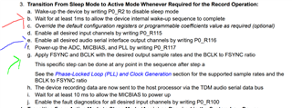
This leads me to believe that the timing of register updates and powering up the ADC and PLL is critical. The Eval board has a lot of delays (10's of mSec) between register writes. It even has a write to register 0x7f which I have not found documentation on.

1) How long after changing PLL registers do I have to wait before Enabling the input channels (register 0x73) or the ASI_OUT_CH_EN (r0x74)?

2) How long do I have to wait after enabling the input channels and ASI_OUT before Updating the PWR_CFG (r0x75) to power up the ADC and PLL?

3) Are there any diagnostics that shut down the ADC that I need to service?

I'm sure I am missing something simple here.

Thanks for your help

Mitch

  • Hello Mitch,

    Thanks for reaching out.

    Before addressing your questions, you say you are waking the part, does that mean the power supplies have already been on and stable and you waking the part from standby or is this in a power on sequence where you wake the part right after supplying power?

    Either way I would monitor power pins for any unusual activity when implementing your procedure.

    Also could you share schematic or tell me of any differences between yours and the evaluation boards.

    Best Regards,

    Carson

    LPA Applications Engineer

  • Carson:

     The power supply is stable. We take the part out of sleep mode and wait 2mSec before writing to any other registers.  Overall the part is functioning. We can get the part to generate I2S clocks correctly.

     The main difference  is we use the SPI interface vs, I2C on the Eval board.

    The issue is that we get no audio data activity on the SDout pin when we use the SPI control interface, but when connected to the Eval board using the I2C interface, it works.

     If you can provide me an e-mail address I can send you a schematic.

     Here are the register settings (in the order sent) we use:

        1. changing the Master clock frequency and the FS0,1 pins. Return this pin high to allow the DAC outputs to operate.

    1. Initialization settings (Page “0” unless otherwise indicated, Format: Register number = Data, both in Hex)

      1. Enable the oscillator (22.579MHz or 24.576MHz).

      2. r0 = 0x00 (page “0")

      3. r1 = 0x00 (Not reset)

      4. r2 = 0x81 (Turn off Sleep mode, as this is the default on power-up).

    Note: Wait for 1 mSec after changing Sleep mode

      1. r7 = 0xBE (Left just, 32 bit, Invert Fsync & BCLK & TX edge)

      2. r0x0C = 0x20 (CH2 I2s on GPIO0, Placed in Right0 position)

      3. r0x0D = 0x40 (CH3 I2s on GPIO1, Placed in Left0 position)

      4. r0x0E = 0x60 (CH4 I2s on GPIO1, Placed in Right0 position)

      5. r0x13 = 0x87 (Master mode, Auto clk Enabled, PLL Enabled, BCLK and LRCLK transmitted, MCLK = 24.576 MHz)

      6. r0x14 = 0x44 (44/48kHz, BCK = LRCLK*64)

      7. r0x17 = 0x20 (Ndiv input = PLL, Pdiv input = GPIO, Bclk divider source = Ndiv Output)

      8. r0x18 = 0x18 (Bclk divider = 24)

      9. r0x19 = 0x08 (Fsync divider = 8)

      10. r0x1A = 0x04 (PLL P divider = 2)

      11. r0x1B = 0x0B (PLL J Multiplier LSB = 0x0B)

      12. r0x1C = 0xE7 (PLL D Multiplier MSB = 0x27, Low bandwidth, High range)

      13. r0x1D = 0x01 ((PLL D Multiplier LSB = 0x01)

      14. r0x1E = 0X82 (N divider enabled, divide by 2)

      15. r0x1F = 0xB0 (M div enabled, divide by 12)

      16. r0x21 = 0x31 (GPIO1 set to drive Secondary I2S data output for CH3, 4)

      17. r0x22 = 0x11 (GPIO2 = Use to drive FS0)

      18. r0x23 = 0x11 (GPIO3 = Use to drive FS1)

      19. r0x24 = 0xA0 (GPI1 = MCLK)

      20. r0x26 = 0x0 Default value! (Set GPIO2,3 for the correct FS0,1 which is: DAC= Single speed mode)

      21. r0x3B = 0xD0 (Default, 8V)

      1. r0x6B = 0x0 (Linear filters, No channel summing, custom IIR HPF filter)

      2. r0x6C = 0x08 (No biquads used, Soft stepping enabled)

      3. r0x73 = 0xFC (Enable CH1-6, [Default value])

      4. r0x74 = 0xF0 (Enable ASI Out channel slots 1-4)

      5. r0x76 = 0xF0 (Clear diagnostic flags, Present in Eval board...)

      6. r0x77 = 0xC0 (Clear diagnostic flags, Present in Eval board...)

      1. p0 = 4 (SWITCH TO PAGE 4)

      1. r0x48 = 0x7F (default value) (HPF IIR filter N0 coefficient)

      2. r0x49 = 0xFD

      3. r0x4A = 0xDB

      4. r0x4B = 0x00

      5. r0x4C = 0x80 (HPF IIR filter N1 coefficient)

      6. r0x4D = 0x02

      7. r0x4E = 0x25

      8. r0x4F = 0x00

      9. r0x50 = 0x7F (HPF IIR filter D0 coefficient)

      10. r0x51 = 0xFB

      11. r0x52 = 0xB6

      12. r0x53 = 0x01

      1. p0 = 0 (SWITCH TO PAGE 0)

      2. r0x7F = 0x0 (Present in Eval board...not defined in docs.)

      3. r0x75 = 0x60 to power up the ADC and PLL after changes are made.

    1. Sample rate settings (Use this register data to change the sample rate)

      1. For 44.1/48 kHz sample rate:

        1. r0x00 = 0x00 (talk to page 0 for the following changes…)

        2. r0x75 = 0x00 (power down everything to adjust registers)

        1. Set xRST0 (PA25) LOW to reset the DAC

        2. Adjust the oscillator between 22.579MHz and 24.576MHz as needed.

        3. Set xRST0 (PA25) HIGH after the Oscillator is running.

        1. r0x14 = 0x44 (Master mode, 44.1/48 kHz sample rate , BCLK = 64*LRCLK)

        2. r0x26 = 0x00 (Set GPIO2,3 for Fs settings of 0,0)

        1. r0x7F = 0x0 (Present in Eval board...not defined in docs.)

        2. r0x75 = 0x60 (Power up the PLL and ALL ADC)

      1. For 88.2/96kHz sample rate:

        1. r0x00 = 0x00 (talk to page 0 for the following changes…)

        2. r0x75 = 0x00 (power down everything to adjust registers)

        1. Set xRST0 (PA25) LOW

        2. Adjust the oscillator between 22.579MHz and 24.576MHz as needed.

        3. Set xRST0 (PA25) HIGH after the Oscillator is running.

        1. r0x14 = 0x54 (Master mode 88/96 kHz, BCLK = 64*LRCLK)

        2. r0x26 = 0x40 (Set GPIO2,3 for Fs settings of 0,1)

        1. r0x7F = 0x0 (Present in Eval board...not defined in docs.)

        2. r0x75 = 0x60 (Power up the PLL and ALL ADCs)

      1. For 176/192 kHz sample rate:

        1. r0x00 = 0x00 (talk to page 0 for the following changes…)

        2. r0x75 = 0x00 (power down everything to adjust registers)

        1. Set xRST0 (PA25) LOW

        2. Adjust the oscillator between 22.579MHz and 24.576MHz as needed.

        3. Set xRST0 (PA25) HIGH after the Oscillator is running.

        1. r0x14 = 0x64 (Master mode 176/192 kHz, BCLK = 64*LRCLK)

        2. r0x26 = 0x20 (Set GPIO2,3 for Fs settings of 1,0)

        1. r0x7F = 0x0 (Present in Eval board...not defined in docs.)

        2. r0x75 = 0x60 (Power up the PLL and ALL ADCs)

  • Hello,

    Okay I see the email you sent and will take look, but what was it you replied to my last post with my email? I deleted my post so it my email wasn't just sitting there but also deleted your reply to it which I didn't mean to do

    Best,

    Carson

  • Our Firware guy had a question:

     We use GPI1 for the PLL clock reference input, but all of your examples use GPIO1. Will this cause any issues?

  • Hello,

    Thanks for the patience I will loop a couple of people more familiar with the device to determine the problem.

    Best Regards,

    Carson

  • Carson:

     I forgot to include the fact that the SPI timing updates registers at a rate of about 2uSec each.

    Thanks

    Mitch

  • Thanks mitch for additional info

    I will make sure to set some time aside to give you feedback tomorrow, as I know Its been pretty slow-going on my part and like to get you feedback.

  • We added delays to each register write and found that this enabled the ASI output data. Now our individual register writes are 73uSec each and the initialization takes about 3mSec.

    After this was done, we found another issue, if we choose sample rates of 88/96kHz or 176/192 kHz, the audio data is heavily distorted and the output level is not consistent. I tried this with both our SPI register writes as well as connecting my Eval board I2C buss to our target and updating registers.

  • I found the source of the distortion. I needed to set r0x73 to 0xf0.The default setting (0xfc) generated by the Pure Path PCM6240  software does not work in our case.

  • Hey Mitch

    Okay great! so what other problems/questions do you still have?

    Best,

    Carson

  • I still need to know the following:

     1) How fast can I update all of the registers on initialization and have the device output Audio data correctly? Currently we take about 3mSec to update 42 registers. Let me know if we simply need a 1.5mSec delay after setting the clock configuration or somewhere else.

     2) What are the ramificatons of changing r0x14 without powering down the ADC and PLL?

     When I did this I found the LRCK changed but then dropped out for 424uSec and then restarted while the SDout dropped out for 1.28mSec. Is this the typical timing of the Auto Resume function?

  • Hey Mitch,

    This might not be as much as a timing issue as it may seem, before I comment anymore I want to make sure you gave a read through of pages 154 and 155 (9.2.1.2 Detailed Design Procedure) to make sure you are using the right mechanism when initializing like the SHDNZ pin. It also talks about timing.

    https://www.ti.com/lit/ds/symlink/pcm6480-q1.pdf?ts=1639949980831&ref_url=https%253A%252F%252Fwww.ti.com%252Fproduct%252FPCM6480-Q1

    Best Regards,

    Carson

    Thanks for your patience

  • We do observe the power up timing. I am more concerned with the fact that we can't write to all of the registers as quickly. All of your examples seem to show the I2C control interface, not the SPI as we are using.

    Any insights into the behavior of the PLL loop settling time as well as ASI buss error recovery would be welcome.

  • Okay,

    Let me see about finding resources for helping with PLL and ASI problems. And apologies between our mismatch in communication but I believe I2C is faster than SPI, especially fast mode I2C.

    Best,

    Carson

  • Hello,

    While I still try find you a more straight forward answer here is additional resource which talks about clocks and PLL, disregard the part number in title.

    https://www.ti.com/lit/an/sbaa382/sbaa382.pdf?ts=1640804340593

    It has been a little slower to get answers during the holiday time of year with coworkers being off. I appreciate your patience.

    Best Regards,

    Carson

  • We are still having issues with the ADC output and the register updates any more details on the register update timing and ASI bus error recovery?

  • Hello,

    Let me see about getting something, I will need to message my colleague who I asked before about this.

    Thanks for your patience,

    Carson

  • One final issue: I can configure the device as a 4 channel ADC and run it at 44/48 kHz as the I2S Bus master given a 24.576MHz clock. When I change the PLL divisors to operate at 88/96 kHz the output is distorted (~20% THD). If I reduce the number of active ADC channels from 4 to 2  the distortion drops significantly. Note: I have 0 biquads /channel, AGC is OFF and the Decimation Filter is set to Linear Phase.

    The White paper:SBAA284 page 5 lists: 4 channels at 192kHz under these conditions.

     It appears that the DSP or the available clock divisors is limiting the performance. Can you offer any suggestions?

  • Thanks for additional detail, I am getting additional assistance

    Best,

    Carson

  • I found that I had to override the Eval board register settings to get it to turn OFF CH5 &6 as well as Turn OFF the AGC to get undistorted audio (Page 0: Reg 0x73 = F0,  0x6c =0). It appears that the AGC_SEL bit is NOT Reserved; Always write 1 to this register bit as specified on the datasheet. The datasheet should also mention that this feature requires DSP allocation that may affect channel count.

  • Can i see your up to date register dump?

      1. Enable the oscillator (22.579MHz or 24.576MHz).

      2. r0 = 0x00 (page “0")

      3. r1 = 0x00 (Not reset)

      4. r2 = 0x81 (Turn off Sleep mode, as this is the default on power-up).

    Note: Wait for 1 mSec after changing Sleep mode

      1. r7 = 0xBE (Left just, 32 bit, Invert Fsync & BCLK & TX edge)

      2. r0x0C = 0x20 (CH2 I2s on GPIO0, Placed in Right0 position)

      3. r0x0D = 0x40 (CH3 I2s on GPIO1, Placed in Left0 position)

      4. r0x0E = 0x60 (CH4 I2s on GPIO1, Placed in Right0 position)

      5. r0x13 = 0x87 (Master mode, Auto clk Enabled, PLL Enabled, BCLK and LRCLK transmitted, MCLK = 24.576 MHz)

      1. r0x14 = 0x44 (44/48kHz, BCK = LRCLK*64)

      1. r0x17 = 0x20 (Ndiv input = PLL, Pdiv input = GPIO, Bclk divider source = Ndiv Output)

      2. r0x18 = 0x18 (Bclk divider = 24)

      3. r0x19 = 0x08 (Fsync divider = 8)

      4. r0x1A = 0x04 (PLL P divider = 2)

      5. r0x21 = 0x31 (GPIO1 set to drive Secondary I2S data output for CH3, 4)

      6. r0x22 = 0x11 (GPIO2 = Use to drive FS0)

      7. r0x23 = 0x11 (GPIO3 = Use to drive FS1)

      8. r0x24 = 0xA0 (GPI1 = MCLK)

      1. r0x26 = 0x0 Default value! (Set GPIO2,3 for the correct FS0,1 which is: DAC= Single speed mode)

      1. r0x6B = 0x0 (Linear Phase decimation filters, No channel summing, custom IIR HPF filter)

      2. r0x6C = 0x10 (No biquads used, AGC OFF, Soft stepping disabled) Note: If set to 08, Distorts due to lack of DSP to support Soft Stepping or AGC for sample rates >48kHz!

      3. r0x73 = 0xF0 (Enable CH1-4, disable CH5-8) Note: If set to 0xFC it distorts @ 88/96 or 176/192k Hz

      4. r0x74 = 0xF0 (Enable ASI Out channel slots 1-4)

      1. p0 = 4 (SWITCH TO PAGE 4)

      1. r0x48 = 0x7F (default value) (HPF IIR filter N0 coefficient)

      2. r0x49 = 0xFD

      3. r0x4A = 0xDB

      4. r0x4B = 0x00

      5. r0x4C = 0x80 (HPF IIR filter N1 coefficient)

      6. r0x4D = 0x02

      7. r0x4E = 0x25

      8. r0x4F = 0x00

      9. r0x50 = 0x7F (HPF IIR filter D0 coefficient)

      10. r0x51 = 0xFB

      11. r0x52 = 0xB6

      12. r0x53 = 0x01

      1. p0 = 0 (SWITCH TO PAGE 0)

      1. r0x75 = 0x60 to power up the ADC and PLL after changes are made.

        Note that this works when using the Eval board to load the register data, but when using the SPI interface, the BLKC and FSYNC outputs are correct but SDOUT and SDOUT2 are not working correctly .
  • Hi Mitch,

    Just wanted to check in and see if you could re-summarize the issue as we can get input from the larger TI audio team. It's a long thread so not entirely clear where you are at with things. Sanjay Dixit from my team will also be following up with you as he has also been supporting ADCs.

    Brian

  • The original three questions remain unanswered:

    1) How long after changing PLL registers do I have to wait before Enabling the input channels (register 0x73) or the ASI_OUT_CH_EN (r0x74)?

    2) How long do I have to wait after enabling the input channels and ASI_OUT before Updating the PWR_CFG (r0x75) to power up the ADC and PLL?

    3) Are there any diagnostics that shut down the ADC that I need to service?

  • Hi Mitch,

    I apologize for the delay. i shall get an answer back to you on jan 27.

  • Sounds good!

     I have more info as well:

     It seems that if you want to use the custom HPF, there is a minimum delay between initializing the part and updating the coef. registers and then the DSP_CFG0 register.

  • The documentation only talks of the following :

    1.Red Arrow in Fig:  1ms after coming out of sleep.

    2.Blue Arrow There is no time delay specified from activation of Input channels to PLL on .

    3. After PLL MicBias it talks of a 10ms wait while MicBiias becomes stable. 

    From your communication it seems that when you slowed down you SPI rate from 2us to 73 us rate the issue was solved.

    Could it be that at Higher rate the bytes are not getting written properly.? It may be an idea to try read back the bytes with the fast rate and slow rate

  • Changing the SPI rate did not fix the issue. When I connected my target board to the PCM6240 Eval board using the I2C connections it worked.

    What seems to work is writing the Custom filter coef data 6.5mSec AFTER all of the other configuration registers were written. I was not able to find any reference to using this filter and it requiring this delay.  I have also tried using the default HPF, but this fails using the SPI bus at these rates.

  • I apologize for the delayed response..

    There is a configuration code on page 155 and 156 of the datasheet. Can you try running just  this sequence with SPI Commands. There is no delay

    mentioned here except a 10ms to enable diagnostics  Do you see digital audio data always after executing this code?

    Please remove  any pullup on SDA and SCL Line. 

  • This configuration is significantly different from what we are trying to troubleshoot. I am trying to get the device to run as a timing master for an I2S audio interface running up to 192kHz sample rates. This example is a slave TDM interface. I can't test this on my hardware at this point.

    I believe that the root cause relates to the initialization of the master mode timing and the configuration of the internal DSP. 

    This example also shows the registers updated in ascending order, so this does not reveal any new sequencing requirements. I suspect this would fail in either SPI or I2C mode without the 1mSec delay after taking the device out of "sleep" mode (writing to register 0x20) that is required (section 8.4.3 Active Mode).

     I tried to use the multiple byte writes in the I2C Monitor on the EVM board to get closer to SPI timing, but there is a limitation to the number of bytes it will send in a single burst (32 or so).  Between bursts there is a 10mSec gap,

     I have found a non-optimal solution that works. I simply hope this information I have shared will save other engineers some time.

    Thanks

    Mitch