This thread has been locked.

If you have a related question, please click the "Ask a related question" button in the top right corner. The newly created question will be automatically linked to this question.

TPA3255-Q1: About heat dissipation structure

Part Number: TPA3255-Q1
Other Parts Discussed in Thread: TPA3255EVM, TPA3255

Hello Support team,

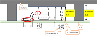
The TPA3255EVM uses the ATS-TI10P-519-C1-R3 heatsink.

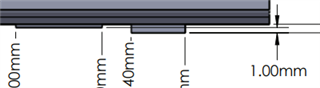
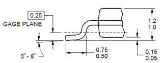
The space where the IC is in close contact with the ATS-TI10P-519-C1-R3 is 1.00 mm.

However, the maximum height of the IC is 1.20mm.

The TPA3255EVM has a structure that puts stress on the IC.

Is there any problem with the same structure in mass production design?

TPA3255EVM User's Guide (ti.com)

ATS-TI10P-519-C1-R3.pdf (digikey.com)

Best Regards.

Kaz

  • Hi Kaz,

    The thermal pad thickness, between top of device and heat-sink, is related to customer structure precision. The thicker, the thermal pad thermal resistance higher.

    The mechanical design is common on customer projects. I think it is no problem.

    Regards,

    Derek 

  • Hi Derek

    The heat dissipation structure of TPA3255EVM is shown in the figure.

    If TPA3255 is max height, I think it overlaps with the heat sink. Is there stress on the IC body, leads and solder part ?

    Is such a heat dissipation design necessary to meet the output power of the specifications?

  • Hi Kaz,

    The thermal pad between heat-sink and top of IC is for deviation of mechanical. On EVM board, it means heat-sink deviation.

    The thermal pad also has thermal resistance. 

    So you should simulation the thermal design according to customer actually application.

    Regards,

    Derek