This thread has been locked.

If you have a related question, please click the "Ask a related question" button in the top right corner. The newly created question will be automatically linked to this question.

OPA1612: opa1612 G=-1 THD degrade.

Part Number: OPA1612
Other Parts Discussed in Thread: PCM1798, OPA1611, PCM4222

i'm using opa1612 to design a single end to differential circuit. schematic as follows.

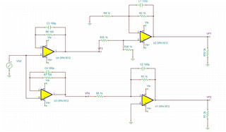
all resistor used in schematic are thin film and caps are NPO.

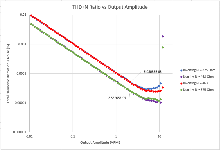
VF3,VF4 have very good thd about -125dbc(1khz, 6vpp sin wave)

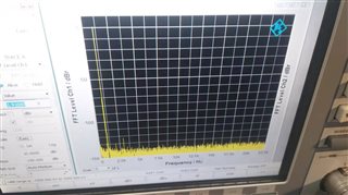
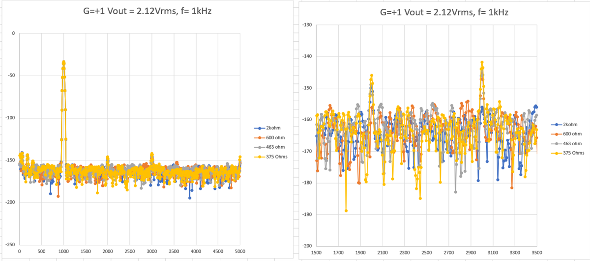
and VF1 has similar thd performance with VF3/4 as U2 operate in G=2 mode.

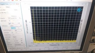
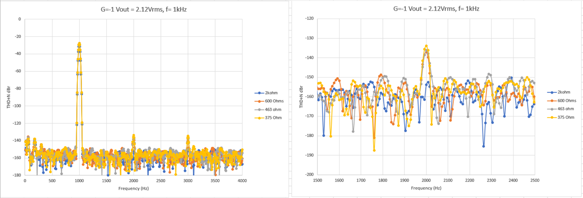
but VF2 thd degrade to -115dbc as U1 operate in G=-1 mode.(HD2 contributes mostly thd degrade, about 10db)

from opa1612 datasheet, G=-1 has slight thd degrade compared to g=1. but below U1 circuit THD degrade a lot. 

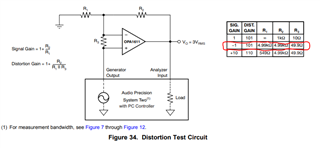
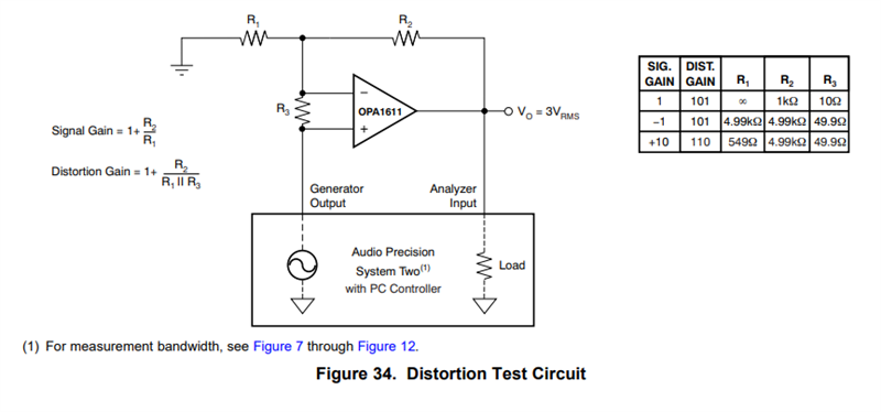
all above thd measure condition is load=600ohm by R&S UPV audio analyzer .

opa1612 supply is +/-11.5V. use soic package.  and i'm wondering whether G=-1 THD performance related it's package. as opa1612 has two package, one is SOIC and the other is WSON package with better thermal performance. 

and i attach G=-1 and G=2 spectrum picture.

can you help to analyze why G=-1 degrade HD2 a lot in above schematic design.

THANKS!

Desktop.rar

  • Hello,

    Can you share screen captures of the spectrum pictures?

  • Jung,

    I am unable to open the .rar file. If you can provide screen captures of the data I can take a look to see if anything stands out. A slight degradation of THD for the inverting case is expected. The non-inverting vs. inverting will have a noise gain difference and closed-loop gain bandwidth differences. 

    I did see your post regarding the PCM1798.  Have you been able to rule out the DAC? It looks like you have made progress from that stage given the -125dbc measurements at Vf3 and Vf4. 

    There are a few things we are considering such as thermal, as well as crosstalk at this frequency. Regarding thermals, the inverting case has an effective load of 375 ohms. This is calculated from Rl = 600 in parallel with R3 = 1k. The non-inverting case has effective load of 461.5 ohms. This is calculated by summing R2 =1k and R4 = 1k in parallel with Rl = 600 ohms. Thermal performance can impact THD as you mentioned. 

    Could you provide the following:

    1) Screen captures of the results.

    2) A full schematic.

    I noticed differences between the Tina schematic and the schematic on the other post. Are you using the dual OPA1612 or the single OPA1611?

  • hi chris,

    sorry i can't share full schematic here.

    left is G=-1,right is G=2.

    I did see your post regarding the PCM1798.  Have you been able to rule out the DAC? It looks like you have made progress from that stage given the -125dbc measurements at Vf3 and Vf4. ------jung replay: yes,rule out DAC. DAC output has a differential to single end circuit and THD about -112dbc in single end

    point(as i posted PCM1798 question, this is because OUT- THD is not good) , then through a 1.5K filter (about 12db suppress to HD2) and THD about -112-12=-123dbc in above schematic VF3/4 point.

    i'm using dual 1612. i also test crosstalk influence as U1/U2 in one OPA1612.  i remove R35 and VF1 output is 0 voltage, then test VF2 point, G=-1 THD has no improve.

    but some other interesting information i can share to you, when remove R35 and U1 works in G=-1 mode , as U1 non-invert input pin2 connected to GND,in theory pin3 also should 0 voltage, but i measured a -100dbc 1khz signal in pin3(VF4 has a 2rms voltage 1khz sin signal).

  • hi chris,

    i have another question, in OPA1612 datasheet, figure 7/8/9/10/11 shows THD+N performance in severlal condition. i want to know these performance is tested only in opa1611 or both 1611 and 1612. 

    i also want to know how TI measure G=-1 THD performance and datasheet "8.3 Total Harmonic Distortion Measurements" shows how to measure THD when G=-1. pls see as follows. but i'm confused to below G=-1 THD measurement, when R1=4.99K,R2=4.99K,R3=49.9.i think this case G=2 not -1? what about your thinking?  thanks!


  • Hello Jung,

    but some other interesting information i can share to you, when remove R35 and U1 works in G=-1 mode , as U1 non-invert input pin2 connected to GND,in theory pin3 also should 0 voltage, but i measured a -100dbc 1khz signal in pin3(VF4 has a 2rms voltage 1khz sin signal).

    This may be a potential ground loop issue in the layout. Does this issue occur on multiple boards?

    I noticed that there are two OPA1612 units in the design. Have you tried exchanging the position of the OPA1612 units? If so, does the issue follow the device or does it occur on the final output of the system? 

    Can you provide us with the Lot codes as well as the Texas Instruments distributor that the devices were obtained from?

    Regarding the datasheet, the gain of -1 is correct. We should have put the inverting equation for the signal gain in the PDS as well. In the gain of -1 case, the signal is applied to resistor R1 while the non-inverting terminal is at ground. This will form the standard inverting circuit with a gain of -R2/R1. 

  • hi chris,

    my board has a ground layer , and  U1 pin3 connected to ground layer by a 0.2mm diameter via. so is it will cause ground loop issue?

    i only test one board at present.

    yes, exchange opa1612, also exchange two opa1611 in one opa1612, same phenomenon. 

    I buy chip from mouser,  and i try to replace by samples from TI(LOT:1228402MY1), no improve to G=-1 THD.

  • Jung,

    The reason we were suspecting a ground loop was because of the signal that is present on the ground plane. The signal measured on the ground plane could have been interference coupling into the probe. 

    The most likely reason for the difference in THD, between the two channels seems to be due to the difference in loading. The inverting circuit is loaded with an effective load of 375 ohms. The non-inverting circuit has an effective load of 461.5 ohms. Does the THD improve on both amplifiers with a 2k ohm load? I would expect the difference between the two channels to improve. Resistors R2, R3, and R4 could also be increased from 1k to 2k as an experiment to see if the THD improves.

    What size resistors are you using? 0402, 0603 etc. Could you provide the part number for the resistors?

    I have boards being delivered next week to try and replicate this measurement.  

  • hi chris,

    you're right, op's THD sensitive to it's load. i'll post a PCM4222 question later.

    when load=2k, G=1 THD improved and G=-1 degrade. so i add a G=1 buffer after VF2 and change R1 from 2k to 200ohm , then output THD of added buffer below -120dbc. this is mt test results, but i don't why G=-1 need a small load, not a big load like G=1? you can try it on your board and see whether same as my test result?

    resistor is 0603 1/10w 0.1% thin film from yageo.

  • Hi Jung,

    I've been discussing this issue with Chris, we can definitely repeat this measurement but need a few more days to get the hardware in place.

    I'm curious, you mentioned you added a buffer to the output of U1, and the THD improved, which makes sense if the load is causing the sensitivity. But you also mentioned you added a 200 Ohm resistor to R1 - but, this would increase the load, since R1 is connected to the output of U1.  Is that right?

    Another thing to keep in mind is that when the load is decreased on U1, there is overall less current flowing on the board and through the supply.  Do you have bypass caps. close to U1, something like a 0.1 uF ceramic?  If the supply has significant variation that is load-dependent, it may also cause problems, and a bypass cap. would help remedy.

    Regards,
    Mike

  • hi Michael,

    some mistake in my above reply , i wrote "G=-1 need a small load means need a small load resistor". and you wrote load decreased means smaller load current, right? 

    yes, R1=200ohm is needed from my test, if remove R1 or increase R1 to 2K, buffer output THD still can not improved to <-120dbc.

    this test results is no match datasheet figure7 as load=2K has better performance than load=600ohm in G=-1.

    i have 0.1uf close to U1.

    thanks!

  • Hi Jung,

    I can't explain why THD is better with R1=200 Ohm. Can you comment more on how you are making this measurement - are you looking at the results from an ADC, or is this feeding directly into a network analyzer? 

    We will try to re-produce here, and hopefully get a THD vs. load curve for the same configuration in the next 2 days.

    Regards,
    Mike

  • hi michael

    ok,thanks!

    in my measurement, feed directly into  a audio analyzer which has a 600ohm resistor load.

    BTW, how do you measure THD?

  • Hello Jung,

    The way we measure the circuit is with the test circuit shown below. We use the Audio Precision in order to make the THD + N measurements. The circuit is in a gain and this gain is calibrated out of the final result. This is done in order to over come the measurement system limitations since the THD of our devices is very good. We need to amplify before measuring. 

    Best Regards,

    Chris Featherstone

  • Hello Jung,

    I will be measuring the THD vs Resistive load tomorrow and will update you with my results by end of the day Friday. 

    Best Regards,

    Chris Featherstone

  • hi Chris,

    thanks your support.

  • Jung,

    I will have to postpone these measurements until the end of next week. I apologize for the inconvenience. I will update this thread with the results once available. 

    Best Regards,

    Chris Featherstone

  • hi Chris,

    sorry to disturb you.

    do you have any update about the test results. thanks!

  • Hi Jung,

    Sorry but Chris is still out of the office.  He will be back early next week.

    Regards,
    Mike

  • Hello Jung,

    I am back in the office. I ran some tests today. I am currently processing the data and will share my results tomorrow. Sorry for the delay. 

    Best Regards,

    Chris Featherstone

  • Jung,

    I have measured THD+N (%) vs Output Amplitude using the equivalent load conditions of your circuit for both inverting and non-inverting gains. The supply voltage is +/-18V. The frequency is 1kHz. The gains I have used are +/-1. For the gain of -1, I am seeing -126dB of THD + N. I calculate this below by 5.08E-7 (5.08E-5%/100) converted to dB.

    Using our test circuit from the product data sheet I see roughly a 6dB difference between inverting and non-inverting. This 6dB difference comes from the fact that for non-inverting we divide the result by 101 or 40dB and inverting by 51 or 36dB. 

    This afternoon I will be measuring the FFT plots instead. This will allow us to see the harmonics themselves and compare against your results. I have marked the position of output amplitude for your condition of 6Vpp or 2.12VRMS. In the plot, within this section the data is noise dominated so it is unclear to me if HD2 is higher for the inverting case. As the amplitude increases further to 10VRMS we become THD dominated and observe an increase in THD with heavier loading. 

    I will update this thread with the FFT plots once I have collected them. 

  • hi  Chris

    thanks very much for your detail test.

    but i can't undrstand you said "This 6dB difference comes from the fact that for non-inverting we divide the result by 101 or 40dB and inverting by 51 or 36dB. ". why non-inverting result divided by 101 and inverting by 51?

    i also want to know something about EVM test dondition.

    1/does EVM OPA1612 power suplly is +/-15V?

    2/from your test, G=-1 THD+N is very good, so the 6Vpp 1khz signal sourced from? and measured by which equipment ?

    3/RL 375ohm and 463ohm are resistive load right? is there any capacitive load?

    4/how opa1612 output connected to test equipment? shield cable?

    5/EVM opa1612 use which package? SOIC or SON?

  • Hi Jung,

    The noise gain is always referenced to the non-inverting terminal. The reason that we divide by 101 or subtract 40dB for non inverting is that the noise gain for non-inverting is 1 in our test circuit. The signal-gain for non-inverting in our test circuit is 1 and the noise source is relative to the non inverting terminal. For inverting the noise gain is referenced to the non-inverting terminal and is 2. The 2 is from the standard non-inverting gain formula since our test circuit is in a gain of 2 relative to the non-inverting terminal. The table in the datasheet has a typo and the inverting distortion gain is 102 not 101. If we divide 102 by the noise gain of 2 we get 51 or 34dB. 

    When we make our measurement using the test circuit in the product datasheet we must factor out the distortion gain in order to get the true THD+N of the device. In doing so we subtract 40dB from our results for non-inverting and 34dB for inverting. This is where the difference of 6dB comes from. 

    In my measurements below I used a supply of +/-11.5V. For the measurements in my last response I used +/-18V supply in order to sweep the output voltage across the full range. The signal source comes from the Audio Precision instrument and is measured back by the Audio Precision instrument at the output of our test circuit shown in the product datasheet. The loads were purely resistive and we used coax cable connections on the input and output of the test fixture. I used the OPA1612 SOIC package. 

    Today I measured the FFT for both inverting and non-inverting cases with several load conditions. My results for HD2 appear to match your results. 

    Inverting: I zoomed into HD2 on the right plot

    Non-Inverting:

    We don't fully understand why HD2 is larger for inverting relative to non-inverting as of now. There isn't really a way to improve upon HD2.