This thread has been locked.

If you have a related question, please click the "Ask a related question" button in the top right corner. The newly created question will be automatically linked to this question.

PCM9211: Using DRX and ADC independently

Part Number: PCM9211

We are trying to replace a digital receiver and an ADC in an existing product with the PCM9211.  At first glance, it appears like it would be a very good fit.  But after digging into the details, I'm not sure if it can do what we need it to do.

Our system configuration looks like this:

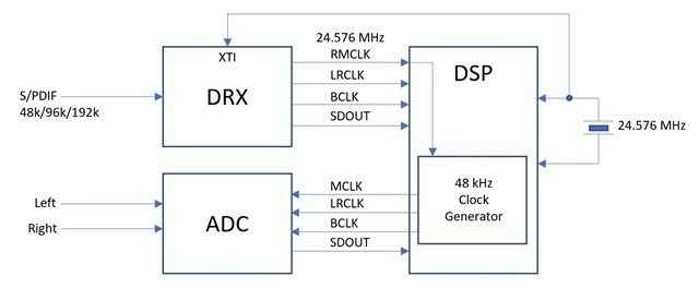
The digital receiver we're currently using always provides a valid RMCLK (Recovered MCLK -- either a recovered 24.576 MHz clock (when the DRX is locked) or the XTI input 24.576 MHz clock (when the DRX is not locked)).  The DRX S/PDIF input can be either 48 kHz, 96 kHz or 192 kHz.  The ADC is a slave, and always runs at 48 kHz.  The ADC clocks are derived from the DRX RMCLK by a clock generator in the DSP, so the ADC is always in sync with the DRX (but possibly at either 1/2 or 1/4 the rate).  If there is no S/PDIF input connected, the DRX is not locked and the 24.576 MHz XTI clock is used to generate the ADC clocks, and in this case the DRX data doesn't matter because there isn't any.

I can't seem to figure out how to do this with the PCM9211.  I found the E2E post that explained that for the ADC to run in slave mode at a particular sample rate, the MCLK must be fed into the XTI input and the ADC configured to clock from XTI.

https://e2e.ti.com/support/audio-group/audio/f/audio-forum/1060685/pcm9211-how-to-use-pcm9211-adc-as-i2s-slave-receive-i2s-clock-from-external-device?tisearch=e2e-sitesearch&keymatch=pcm9211#

And from the PCM9211 datasheet section 7.3.1:

"When the PLL is locked, the secondary clock source automatically selects the PLL clock (256fS). Otherwise, the XTI clock source is selected. Register 32h should be used for dividing in the lock status (that is, the PLL source). When unlocked, Register 33h should be used (the XTI source)."

It seems like this is a "chicken or egg" problem.  The SCKO is either the PLL clock or the XTI clock.  But the XTI clock needs to come from the DSP clock generator (which uses SCKO as its input) to run the ADC in slave mode locked to the SCKO clock.  That isn't going to work.

So I'm a little confused as to what to do here, or if there is evan a way to do what I'm describing with the PCM9211.  Any insight would be very much appreciated.

Thank you!

-Dan

  • Hello Dan,

    From what I understand from your block diagram, it seems to me it is what data sheet is showing as simplified application diagram . You are using a 24.576MHz crystal osc and  you can feed that to XTI  (crystal resonator or external XTI clock source input)  and set up the internal PLL and dividers  to generate ADC Clock (SCK /BCK/LRCK) and XMCKO. Basically the clk inputs to  ADC in your diagram that are coming from DSP  are internally generated.

    Regards,

    Arash

  • Hi, Arash.

    What still isn't clear to me is whether the ADC will be clocking from XTI or from the DRX recovered clock when the DRX S/PDIF input is plugged in.  We need the ADC data to be locked to the DRX data when it is present.  If the PLL is recovering the clock from the incoming S/PDIF signal, will the ADC be using that recovered clock or the XTI 24.576 MHz clock?

    Thank you,

    -Dan

  • Dan, ADC can be configured to use a specific clock by setting  ADCLK[2:0] register (Register 42h) appropriately. Please refer to  "7.3.8.5.2     ADC: Clock Source Configuration"  section. Is it what you are asking?

    Regards,

    Arash

  • Yes; I believe that register allows the ADC to be configured to clock from AUTO (DIR (locked) or XTI (unlocked)), DIR, XTI or AUXIN0-2.  But I want to clock the ADC as a slave from the DSP LRCLK/BCLK/MCLK outputs, as shown in my original diagram.  The E2E thread here:

    https://e2e.ti.com/support/audio-group/audio/f/audio-forum/1060685/pcm9211-how-to-use-pcm9211-adc-as-i2s-slave-receive-i2s-clock-from-external-device?tisearch=e2e-sitesearch&keymatch=pcm9211

    explains that the MCLK has to go into XTI for ADC slave mode.  But if I do that, I have a circular clock path. XTI -> SCKO -> DSP -> MCLK -> XTI.  The DIR case isn't circular (PLL -> SCKO -> DSP -> MCLK -> XTI), but it does assume the PLL can lock (and the part can run at all) without a stable clock on XTI.

    The diagram you refer to is likely operating the ADC at the DIR rate, which is not our use case.  In our system, the ADC always runs at 48 kHz.  The DIR S/PDIF input can be at 48, 96 or 192 kHz, so the ADC and the DIR aren't always running at the same rate (though, they will always be at an exact ratio of 1/1, 1/2 or 1/4 (48/48, 48/96 or 48/192)).  That's why the DSP uses the recovered MCLK from the DIR (or a 24.576 MHz XTAL, when the DIR isn't locked) to generate a constant 48 kHz clock to the ADC that is locked to the DIR rate (or a 24.576 MHz XTAL, when the DIR isn't locked).

  • Daniel, Let us take a closer look at it and will get back to you  by the end of the week.

  • Thank you, Arash!

  • I just found another E2E post:

    https://e2e.ti.com/support/audio-group/audio/f/audio-forum/744144/pcm9211-configure-pcm9211-adc-as-i2s-master-via-mpio_c

    that describes running the ADC MCLK into MPIO_C0, AUXIN1.  This could be a possibility.

    But the next problem is that we've been trying to figure out how to make the secondary port (MPIO_A) clocks work as described in the datasheet, where they are generated by the PLL when the DIR is locked and by the XTI when the PLL is not locked.  We need valid clocks whether the PLL is locked or unlocked.  Other digital receivers we've used have the ability to switch automatically from the PLL to crystal-generated clocks when the PLL is not locked.  The datasheet seems to indicate this is possible with the PCM9211 as well, on the MPIO_A secondary clocks.  But what we are seeing is that the MPIO_A secondary clocks seem to be inverted from the main output port clocks, and the LRCK seems to also be shifted as well.  And when the DIR is not locked, both the main output clocks and the MPIO_A secondary clocks drift down to a very low frequency (presumably following the PLL).  The secondary clocks on MPIO_A don't switch to the XTI clock source, as described in the datasheet (section 7.3.1):

    "The PCM9211 also has two output ports for the DIR output. The primary output is available from the Main Port
    and/or MPIO_B; the secondary port is available through MPIO_A. The dividing ratio of BCK and LRCK for the
    primary output is defined by the DIR. The dividing ratio for the second output (normally taken from MPIO_A) is
    defined by Register 32h and Register 33h.

    When the PLL is locked, the secondary clock source automatically selects the PLL clock (256fs). Otherwise, the
    XTI clock source is selected. Register 32h should be used for dividing in the lock status (that is, the PLL source).
    When unlocked, Register 33h should be used (the XTI source)."

    We are currently making the following changes to the default register settings:

    w 80 24 10
    w 80 26 81
    w 80 27 10
    w 80 2f 05
    w 80 30 14
    w 80 31 0a
    w 80 48 21
    w 80 6e 00
    w 80 6f 80

    Is there another register setting we're missing to make the secondary clocks work as described above (switch to XTI clocks when PLL not locked)?

    And is it expected that the secondary clocks don't match the main port clocks when the PLL is locked?

    Thank you!

    -Dan

  • Hi Daniel, 

    I am looking at this at the moment. I shall try to revert tomorrow 

  • Is it that you like to interface the PCM9211 with the existing firmware in the DSP?

    The ADC Has a Standalone mode where it can receive external clocks over MPIO_C from your DSP and can be a master or a slave.

    Would this somehow be an option for you?