Hi Sir,
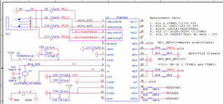
Arrange measurement data as follows,
1. In MD6/MD5/MD2 (000) SE Ch 1 (VINL1 and VINR1) mode
2. Pin 6 (VREF)/C17=1.65V & Pin 11 (LDO)/C29:=1.95V
3. Pin16 (LRCLK)/R24=48Khz & Pin 17 (BCK)/R25= ~3.07Mhz
4. Pin 18 (SDOUT)/R26: No dataoutput ~ 0V?
5. Pin1 (VINL2/VIN1M), Pin2 (VINR2/VIN2M) and Pin27~30 DC Bias are 1.65V
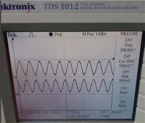
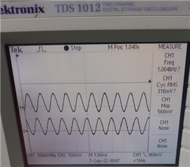
6. The DC Bias of Pin3 and Pin4 drifts unstable from 0V to ~1.4V, and waveform as below pictures.


The current question is why the DC bias voltage of pin3 and pin4 is unstable, and there is no signal output from the I2S data pin?
Need your help!
Thanks,
Tom


