Other Parts Discussed in Thread: TAS5414C,
Hi,
I am trying to build the TAS5414C evaluation board, which I would also like to use as a normal amplifier. I found multiple schematics and documents related to this.
Option-1. TAS5414CQ1PHDEVM Eval board, under Hardware development
Option-2. ASSEMBLY DRAWING, under Design & Tools simulation.
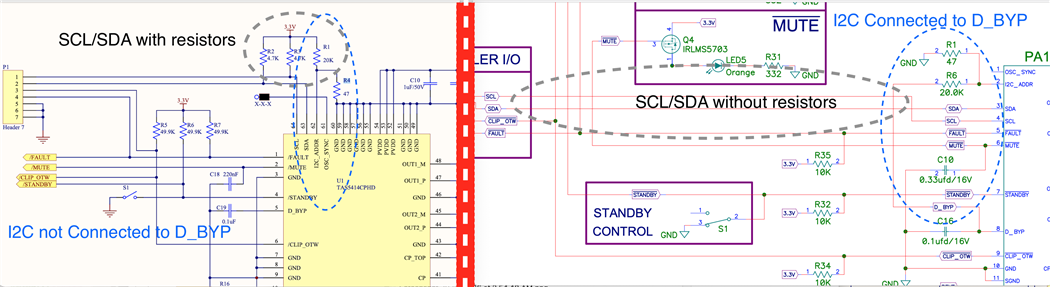
Tho. much of a design in mostly identical, but there are still few differences e.g at power side, 4 33uF capacitors are used in Option-1 while only 2 are used in Option-2.
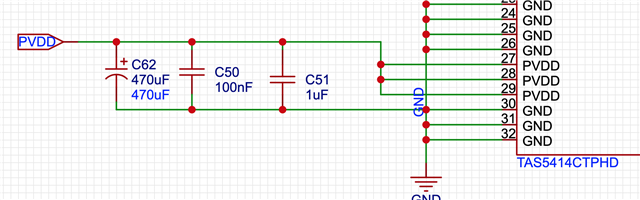
For PVDD, 2 1uF/50V capacitors are used in Option-1 while 0.1uF/50V capacitor is used in Option-2.
My question is, which sciatic should I follow? Option-2, as date-wise its recent one.
My other question is, what design changes are required to get 79W/Ch? As Option-1 states that the input is 12V.
As per data sheet options,
– 28 W/Ch Into 4 Ω at 14.4 V
– 50 W/Ch Into 2 Ω at 14.4 V
– 79 W/Ch Into 4 Ω at 24 V
I may need to provide 24V input. Is that sufficient or are there any additional changes required to the schema?
Regards
-Mayuresh