This thread has been locked.

If you have a related question, please click the "Ask a related question" button in the top right corner. The newly created question will be automatically linked to this question.

TPA2011D1: Analysis of the scalding problem in the application of bone conduction earphones

Part Number: TPA2011D1

A, Application Description

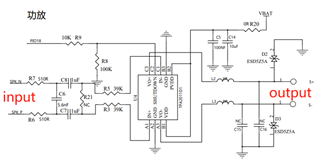
Input: Class D output signal connected to Qualcomm QCC3040 Bluetooth chip

Output: bone conduction sound unit connected with 8 Ω impedance.

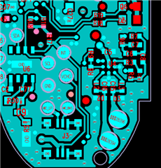
The corresponding PCB layout is as follows:

B, Problem feedback

Shipped 10k+, customer complained 20+

All customer complaints are sound unit burning


C, Analysis and confirmation

  1. Confirm with the sound unit supplier that the condition for scalding is that DC voltage is applied to the positive and negative poles.
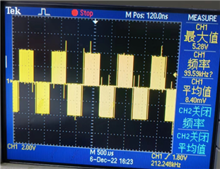
  2. We have conducted destructive tests. When 2.0V DC voltage is applied to both ends of the sound unit, it starts to burn, and the temperature can reach above 50 ℃.
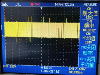
  3. We tested the defective products returned by customers and found that there was about 2.7V DC voltage at both ends of the sound unit.
  4. We also found that the 2.7V DC voltage disappeared after the EN pin (C2) was grounded, which basically judged that the output DC voltage was from TPA2011D1.


D, The help and support we need

  1. How does TPA2011D1 output pin generate DC voltage?
  2. If it is a design problem, how do I modify it?
  3. Production is continuing, and we need to solve it as soon as possible to reduce losses.

Best regards.


  • Hi Zero,

    I think this same application came up to the forum some time ago but discussion didn't continue.
    Can you try by adding a filter at the output, ie. populate L2, L3, C15 and C16?
    You must consider that TPA2011D1 is a Class-D amplifier, thus the output signal is a fast switching PWM, usually for normal speakers this kind of signal is not a problem, as the offset is cancelled due to BTL (differential) connection to the speaker. However if this specific actuator is more sensitive to these signals, then you may need to use the filter.

    Best regards,
    -Ivan Salazar
    Applications Engineer

  • Hi Ivan,


    Adjusting the output filter will cause the sound to change. No suitable filter has been found.

    In addition,

    After testing, we found that the DC voltage at TPA2011D1 output terminal was caused by a faulty square wave signal, and the waveform was all above the zero point, as shown in the figure below.


    In the normal prototype test, the waveform is distributed on both sides of point 0, as shown in the following figure.


    So I think it is not that there is no filter circuit that causes the sound unit to burn, but that there is something wrong with TPA2011D1, and I don't know what is wrong?


    Best regards.

  • Hi Zero,

    Sorry for the late response, somehow your post got out of my dashboard and I lost track.

    I have a few questions on these scope captures:

    • The scope shows only CH1, does that mean a single output is producing both positive and negative? How are you measuring the output?
    • What are the LC component values you've tested

    Best regards,
    -Ivan Salazar
    Applications Engineer

  • Hi Ivan,

    I test the signals at both ends of the load. Connect the probe of the oscilloscope to the S+ and S - test points in the figure below.

    Wherein, C15 C16 is NC, L2 L3 is 0R, and D2 D3 is ESD diode.

    When I play the sound signal, the waveform measured at the load end, because TPA2011D1 is a mono power amplifier, there is only one channel waveform CH1.

  • Hi Zero,

    Thanks for the details, I understand you're measuring across both outputs as opposed to measure from each one to GND.
    A couple things to check further:

    • Do you have an estimate of how many units show each type of output?
    • Instead of measuring with a single channel across S+/S-, can you test by using two channels, one from S+ to GND and the other from S- to GND? Please use an RC or LC filter so we can see the analog signal without the fast Class-D switching.

    Best regards,
    -Ivan Salazar
    Applications Engineer

  • Hi Ivan,

    Thank you for your reply.

    We will send you the waveforms from S+ and S - to GND after testing, and we can also test them by adding filters, but do you have good recommendations for RC or LC parameters?

    • Do you have an estimate of how many units show each type of output? ---》I don't understand this sentence. Can you explain it again?

     Best regards.

  • Hi Zero,

    I mean how many devices show each type of output? You shared two different output results:


    In the normal prototype test, the waveform is distributed on both sides of point 0, as shown in the following figure.


    I've requested some EVMs of this device to double check the outputs on my side as well. I may be able to test some of them over next week.

    Best regards,
    -Ivan Salazar
    Applications Engineer

  • Hi Ivan,

    The above figure is the waveform of the output error, which is tested from the defective products.

    The defective products were fed back from the market consumers, and no such defective products were found at the production end of our factory.

    At present, the sales volume is about 20000 pcs, and the defective products fed back by consumers are about 30 pcs.

    Waiting for your test results, thank you.

    Best regards,

  • Hi Zero,

    Thanks for the details, perhaps the returned devices got damaged somehow and thus showing this abnormal behavior?
    I'll let you know test results next week, although I would expect similar results as your factory production line.

    Best regards,
    -Ivan Salazar
    Applications Engineer

  • Hi Ivan,

    We have checked and confirmed that the customer found the fault just after receiving the prototype and returned it the same day, which can eliminate the man-made damage.

    Best regards,

  • Hi Zero,

    Thanks for the notice. I'll try to track these in our system to check if they were tested already.

    Best regards,
    -Ivan Salazar
    Applications Engineer