Other Parts Discussed in Thread: PCM1822-Q1
We need to make sure our PCM1821 (or PCM1822-Q1) board is as quiet as possible, but the system we're connecting to is fairly noisy. Thus we want to isolate our analog signals, power, and GND as much as possible from that noise.
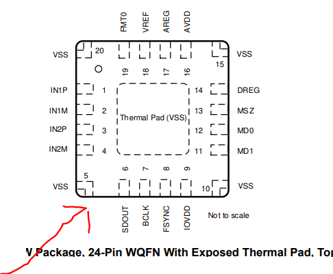
The datasheet pinout identifies all GND pins as "VSS", though some have type "Analog supply" and some "Ground supply". The layout guidelines suggest making sure that the thermal pad is connected to GND with a via pattern connecting straight to the board's GND plane. They also indicate VREF's capacitor tie to AVSS without vias.
Questions:
- Is it best to separate the thermal pad VSS from the Analog supply VSS pins, with separate analog and digital GND planes, or solidly tie them to a single GND? (It's not super clear to me from the datasheet)
- Does the answer to #1 change if the system GND you're tying into is quiet or noisy?
- If we separate AVSS and VSS, is there an ideal point in the PWB to link them together?
- It's a little strange that FMT0 is a digital input, but is referenced to the AVDD supply voltage. Is this a potential source of noise in our system if we want to ground FMT0, especially if our VSS is noisy?
- If so, should we connect FMT0 to AVSS or VSS?
- Will the resistance we choose for tying FMT0 to AVSS or VSS make a difference in noise in the ADC?
Thanks in advance!
Chris