This thread has been locked.

If you have a related question, please click the "Ask a related question" button in the top right corner. The newly created question will be automatically linked to this question.

SRC4392: DIR, PLL1, & 98.304MHz

Part Number: SRC4392
Other Parts Discussed in Thread: ADS127L01

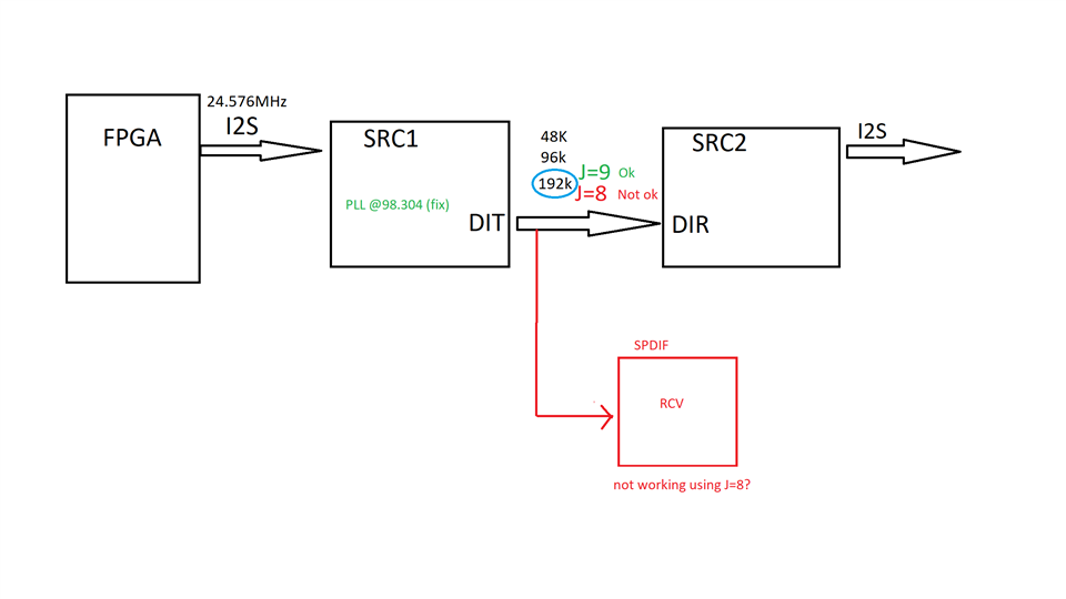
I have 2 SRC4392 running off the same 24.576MHz MCLK. 

  1. Port A (192kHz I2S slave) => SRC => DIT (48kHz, 96kHz, or 192kHz)
  2. DIR => SRC => Port A (192kHz I2S slave)

I have PLL1 configured as recommended in the DS (P=2, J=8, D=0) to get 98.304MHz.  Everything works great at 48kHz and 96kHz, but at 192kHz, the lock is sporadic and the received channel status jumps all over; sometimes correct and sometimes random. 

If I change the PLL1 to 110.592MHz (P=2, J=9, D=0), 192kHz audio appears to work.

The DS states

Registers 0x0F through 0x11 are utilized to program PLL1 in the DIR core. PLL1 multiplies the DIR reference clock source to an oversampling rate which is adequate for AES3 decoder operation

and then provides calculations to get as close as possible to 98.304MHz. 

Is this a magic frequency with consequences if PLL1 is set to another frequency?

Thanks,
Jon

  • Hello Jon,

    The DIR reference clock can be any frequency that meets the PLL1 setup requirements : (CLOCK × K) / P = 98.304MHz. So this frequency is internally set and you choose the coefficients based on your reference clk to meet this requirement. Note that datasheet recommends that " the clock sources for MCLK and RXCKI input be generated by low-jitter crystal oscillators for optimal performance. In general, phase-locked loop (PLL) clock synthesizers should be avoided, unless they are designed and/or specified for low clock jitter.

    I guess your modified coefficient is a better fit for the actual clk that it sees in order to fit in the equation given above.

    Regards,

    Arash

  • The datasheet is not clear that 98.304MHz is a requirement.  If very strongly implies it by having a table with suggested multipliers to achieve 98.304MHz and resulting errors, but the statement

    PLL1 multiplies the DIR reference clock source to an oversampling rate which is adequate for AES3 decoder operation

    Also implies the specific frequency is not important, only that it is high enough to allow for the needed oversampling.

    My clock signal is directly from a 50ppm crystal resonator, so accuracy and jitter on the clock should not be an issue.

    I believe I have found the source of the problem (variable stream signal path degradation) which is making the DIR loose lock.

  • I agree, datasheet mentions 98.304MHZ only in that equation and no other explanation.  This part being a mature part,  I was not able to find any other documents for this part.

    It is good you have found  signal path degradation was the source of the problem, if you have any more findings it would be great to share it here.

    Regards,

    Arash

  • Hello ,

    was it really only the input signal degradation?

    About 3 years ago I tried to get 192 / 200 kHz (all lower fs okay) to work without success. Only with individual PLL tuning I could make it work, but if I changed the input source (with some ppm clock difference to the previous) I had to tune it again, so it was useless for my application.

    Right now our currently used CS8422 was just set to end of life, so I'm lokking at the SRC4392 again - maybe someone else found something that I didn't.
    By datasheet it should work, but it didn't...

  • Hello Christian, I believe the issue is related to your clks. I recall I worked on one SRC devices that was working fine for all frequencies when I was using the PLL on the EVM, but when using external SCK it had issues with higher frequencies . I remember adding some random jitter in AP (my clk source) resolved the issue. 

  • Hello Arash,

    thanks for your hint - but how can that be?

    In my use case (FPGA is I2S master providing all the clocks) SCK is "only" the I2S bit clock, I am pretty sure that the SRC4392 fails on the SPDIF receiving side, as my tests with PLL1 registers have shown. For each individual SPDIF source and for each individual SRC43 and for every combination I got it to work only by tuning the PLL1 registers - which is unusable if you have an unknown source.

  • Hello Christian, 

    Assuming reference clk is  a stable   24.576MHz, with J=8, it should work-

    Have you captured the clks and compared the edges relative to each other for both cases of J=8 and j=9,  to find some hints or data point?

    Would you add any missing information (or do any correction to the diagram below) just we have the correct picture of the application and issue.

    Arash

  • No, it's like in the picture above.
    And again:

    - this is part of a multi-channel system

    - all other channels working perfectly, clocks are really clean and low jitter

    - power supply is super silent

    - SPDIF input signals look very good, also at 192k & 200k

    - using CS8422 instead of SRC4392 works perfectly at all sample rates

    - problem only occurs when SPDIF sample rate is 192 kHz or 200 kHz

    - only individual tuning of PLL1 helps, depending on source and system clocks (25ppm difference between systems)

    BUT: individual tuning is out of the question, so until now the SRC4392 is unusable for us

  • Thanks for sending these info , let me take a look at it and also discuss it with my colleague and will get back to you by Tuesday.

    Regards,

    Arash

  • Would you please clarify  when you say " it is a part of multichannel system and  all other channels working perfectly"  do you mean only one channel is problematic at 192K and other channels are okay at 192K?

    We can't really tell for sure what is going on inside the path from PLL1 to  PLL2 to .... If individual tuning is out of the question for you , here are few suggestions to debug further:

    The maximum available  output clock rate for PLL2  for a given input sampling rate is estimated by internal logic. It can be read  at register 0x13. Also check pins 11 and 12. The lock output (pin 11) is active only when both the AES3 decoder and PLL2 indicate a lock condition. You might need to monitor some more GPO pins from Table 1. 

    One suggestion or test is to run FPGA at higher frequency (x2) and see if it works for 48k,96K and 192K. Our guess is it should work without the need of PLL tuning for 192K. With same token, reducing your input clock from 24.576MHz to half,  most probably would cause the fs of 96k not work as well.

    Regards,

    Arash

  • Hello Arash,

    thanks for taking care of this!

    Multi-channel system:

    - the system is kind of modular audio system with several slots for "stereo modules"

    - these slots are equipped with analog input modules (24bit ADCs, ADS127L01) and / or
      digital input modules for optical SPDIF input (until now using the CS8422)

    - the complete system is running with sample rates up to 200 kHz

    - the FPGA is the clock master for I2S with the same clock lines (with termination) going
       to all modules

    - basic clock source are low jitter oscillators

    - the existing channels (and oscilloscope measurments) show that our clocks are clean
       and stable, we easily reach the ADC's specs, as well as the CS8422's specs for noise
       and THD

    So, regarding your suggestion to use a higher MCLK, that is not possible, because at 25.6 MHz
    we are already close to the SRC's maximum of 27.7 MHz.

    Our clock rates on the I2S side, provided by the FPGA:

    fs = 200 kHz, MCLK = 25.6 MHz
    fs = 100 kHz, MCLK = 25.6 MHz
    fs = 50 kHz, MCLK = 25.6 MHz
    fs = 25 kHz, MCLK = 12.8 MHz

    fs = 192 kHz, MCLK = 24.576 MHz
    fs = 96 kHz, MCLK = 24.576 MHz
    fs = 48 kHz, MCLK = 24.576 MHz
    fs = 24 kHz, MCLK = 12.288 MHz

    As by the SRC4392 datasheet, this should not be a problem, also concerning the oversampling ratios.

    And again, for all sampling rates on our system's / the I2S side, SPDIF signals at 192 or 200 kHz
    only working stable with fine tuning of PLL1.
    Checking the registers and dedicated pins (#LOCK, #RDY) confirm that it's a PLL1 problem.

    It's so frustrating, all is working well, only at 192k/200k it's failing.

  • Thanks Christian, 

    We were thinking either to go higher or lower in frequency to see the effect at 192k or 96k, since going higher is not feasible for this part, may be going lower can give some insight with 96k sampling frequency. 

    One thing that you may want to check is  that in Slave mode, the ports do not require a master clock, as the LRCLK  and BCK are inputs that are sourced from the external audio device serving as the serial bus timing master. So  you might want to  remove the Master from port  and see. 

    We don't have a board to test this here but even with our EVM we might not see this  problem. If you wish you can send us your board and we can try it at our end and see what we can find.

    Regards,

    Arash

  • Hello Arash,

    > ... that in Slave mode, the ports do not require a master clock, as the 
    > LRCLK  and BCK are inputs that are sourced from the external audio
    > device serving as the serial bus timing master.
    > So  you might want to  remove the Master from port  and see. 

    If I understand the datasheet correctly, then maybe the I2S port does not need the MCLK, but the DIR / PLL1 needs some reference clock, which in my case must be MCLK (datasheet page 31, 2nd paragraph), or MCLK is physically routed to RXCKI.

  • Btw, are there any other SRCs with SPDIF input which are using a different "SPDIF receiver front-end"?

    I played again with the PLL1 settings, and as soon as I find the right settings it works - but again, only for that particular input signal. 

  • The SRCs that we have are  mature devices designed many years ago  and I can not tell you whether they are using a different front end or not. My guess would be they  use the same SPDIF receiver front-end.

    https://www.ti.com/audio-ic/interface/sample-rate-converters/products.html

    MCLK is not physically routed to RXCKI and  as it is shown in the block diagram of fig 67 you need either of them for PLL1 .

    Regards,

    Arash  

  • Okay,
    I just put a wire from MCLK to RXCKI and chose RXCKI as PLL1 input, same behavior.

  • That is strange, The only thing that I can suggest is to send your board to us  and let us see if we can figure out the issue with the system.

    Arash

  • Hello Arash,

    okay, where can I send these boards to?

    And what info do you need?

    It is on a 70mm x 48mm PCB with 2mm header pins.

    The I2S audio clocks& data are on these pins.

    The I2C control is connected to an on-board ATmega, but via 2 serial resistors so it could be accessed.

    But I would only send in a module if someone really made the effort of looking at it - closely...

  • Hi Christian,

    I will leave the office shortly and will come back on the 17th of July. So if you want  wait until i come back

    I will work on it as my schedule permits,  so it might take a while but I don't promise that I can solve the issue, as I think you already pretty much checked everything, but I can give it another try. 

    If you choose to send it,   I need several pictures of your set up  along with any script to be  loaded  into any generic I2C master so I can get the set up to run with least amount of trouble.

    Also if there are special cables that you think might be useful to send along, please do so.

    Regards,

    Arash