This thread has been locked.

If you have a related question, please click the "Ask a related question" button in the top right corner. The newly created question will be automatically linked to this question.

TLV320ADC6140: FSYNC / BCLK edges timings

Part Number: TLV320ADC6140

Hello,
I'm using TLC320ADC6140 in slave mode connected to a STM32 processor. TDM mode, 2 slots of 32 bits, no TX offset, default polarity for FS, BCLK. FSYNC rate 48kHz and BCLK 3.08MHz.
Firsts test work fine, I get the result expected.

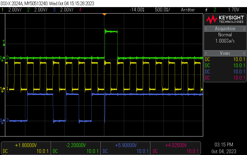
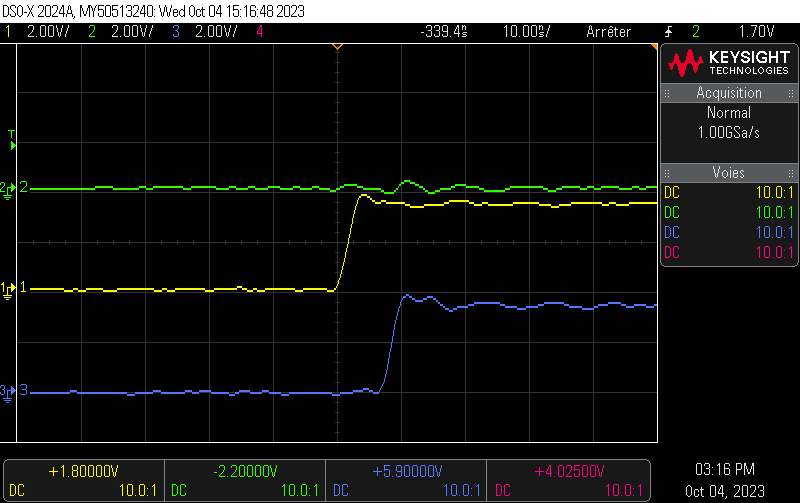
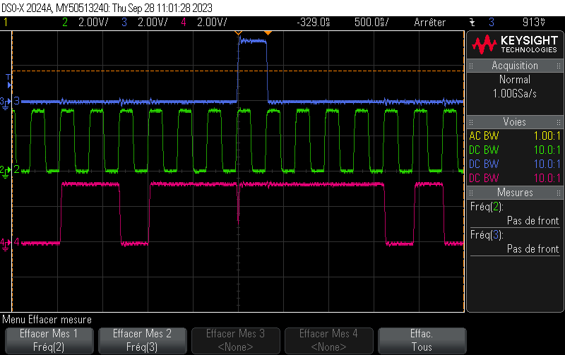
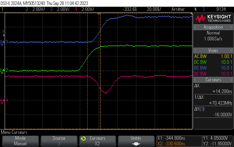
On the scope screen, we see that FSYNC rise about 15ns after BLCK edge. We can see on the screen that the TLV starts updating its output to a 0 (void fill) on the BCLK edge, but 15ns later, while the DOUT signal is still falling to 0, the FSYNC edge comes and the output is immediately updated with the MSb value of slot 0.
Blue = FSYNC, Green = BCLK, Red = SDOUT.
We can read in section 8.3.1.2.1 :
"In TDM mode, also known as DSP mode, the rising edge of FSYNC starts the data transfer with the slot 0 data first. {...} FSYNC and each data bit (except the MSB of slot 0 when TX_OFFSET equals 0) is transmitted on the rising edge of BCLK"
It says that the SDOUT signal is updated on the rising edge of BCLK, except for the MSB of slot 0, but without more explanation. It seems that the rising edge of FSYNC overrules the BLCK edge and forces SDOUT update, am I right ?

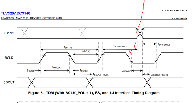
But I'm not sure of the margin I have on the FSYNC / BCLK edges timing. The TLC datasheet does not provide a lot of chronograms, and the only one for TDM mode is given for BCLK_POL = 1, and I'm not sure how it is linked to FSYNC edge in my config with BCLK_POL = 0.
What happens if the FSYNC edge comes too early after BLCK edge or is seen before BLCK edge (devices or layout tolerances) ? Is there a risk of loosing the MSB of slot 0 (that would be transfered on FSYNC edge, but replaced by the next data bit on the very next BLCK edge ?
Should I be in a more safe condition if I add a small RC on FSYNC to ensure minimum delay between BCLK rise and FSYNC rise (I already have 100R+22pF on each line) ?

Thank you
Aurelien

  • To begin I would suggest to try taking all measurements by putting a 22 ohm series resistor on BCLK DOUT and FSYNC . No capacitance is needed

  • Hello,

    I don't see what kind of information I could expect from changing the resistors on all lines. That would only results in a faster slopes, but the timings will be the same (we see that FSYNC is driven ~15ns after BCLK edge).

    I just need to understand how the edges are handled in the ADC, and what would happen if the delay between the two edges is smaller or even if the order of edges is inverted.

    Aurelien

  • The Datasheet  specified a time Td(Fsync) 

    While this spec is for master mode it can be used for Salve mode also. Would there be a chance that your system can go to BCLKPOL =1. ?This uses the Falling edge of BCLK to get data. If you do that the switching edge of BCLK is seperated from the RISING  edge of FSYNC.

    Also, We normally suggest 22 ohm series resistances close to the source of The Digital outputs. No capacitor is normally used.

  • Hello,
    I'm not sure that switching to BCLK_POL = 1 will help, because it just inverts the clock, but the questions I have about BCLK rising edge and FSYNC rising edge with BCLK_POL = 0 (data is updated on the SDOUT on BCLK rising edge and FSYNC rising edge), will be exactly the same with BCLK falling edge and FSYNC rising edge (data will be updated on BCLK falling edge and FSYNC rising edge), as shown on figure 26.

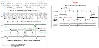
    I made a quick picture merging the timings of the datasheets with the min/max values. It's not easy at a glance to compare both timings because of the BCLK and FSYNC polarity differences choosen for the illustration.


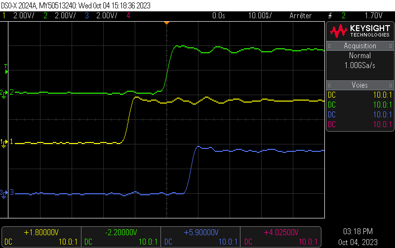
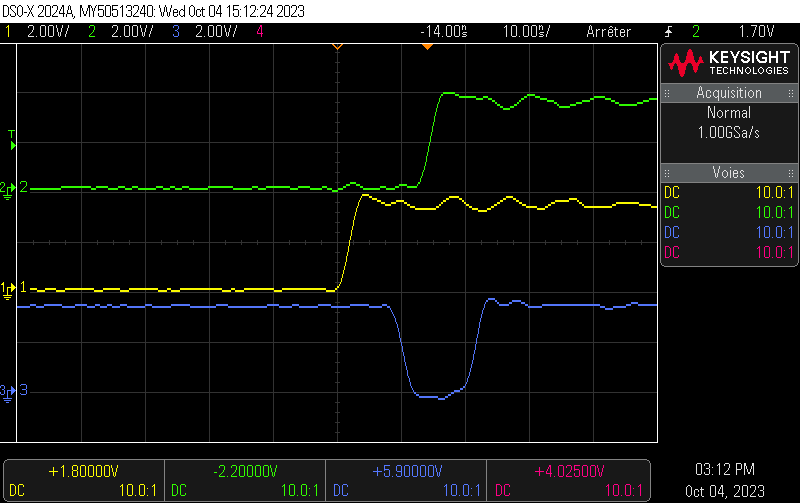
    Below are some measurements of the signals measured with Rs=22R for all lines and no BW limit on scope.

    General view :

    BCLK to SDOUT in middle of frame : 

    FSYNC to SDOUT without glith : 

    FSYNC to SDOUT with glith due to previous BCLK edge : 

    Do you confirm everything is ok ?

    Thank you

    Aurelien

  • I am speculating here: may be incorrect

    After 8ns(TSU FSYNC) from the rising edge of FSYNC Data from the MSB is enabled.

    It seems to me that the last rising edge of BCLK in the frame writes a 0. About 8ns after the rising edge of FSYNC the MSB replaces this bit. The risk here may be that the last bit of the frame may be present for a very small time for the SOC to read it.

    There is a I2C bit called TX_Edge

    A 1 on This bit should shift the latching of the data to the falling edge of BCLK. I am thinking that Data output should appear at the points indicated by the red arrows.This would then give a substantial time for the last Data on the frame .

    Perhaps toggling this bit can be tried.

  • Hello
    I think there is a misunderstanding about this glitch.
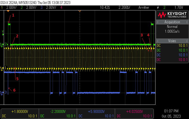
    I captured a full frame, sorry for resolution, its the scope, but it's good enough to understand the whole picture.

    1. The SDOUT data is updated on the rising edge of FSYNC with the MSB of 1st slot
    2. The next bit is updated on the next SCLK edge
    3. This is the SCLK edge that updates SDOUT with the LSB of 2nd slot
    4. This SCLK edge updates the output with a "0", and it is always a "0" that is sent here, it is not a data bit, it is a "0" bit because I configured the ADC to force 0 (and not Hi-Z) on SDOUT on exceeding clock cycles.
    5. My MCU interface samples the data on the falling edge of SCLK (I made an error with the position of the arrow, it points to a rising edge while I'm talking about the falling edge here !)
    6. We see the glith on the SCLK rising edge just before FSYNC rise and triggers the update of SDOUT with MSB of first slot. That glitch is always at 0 level, as explained in point 4

    So I don't loose any data and the glitch is unseen by my MCU interface...

    Aurelien

  • Since your MCU Captures data on the Falling edge of BCLK you should be fine.