Other Parts Discussed in Thread: PCMD3140
Dear All:
There is a audio project based on pcmd3180 device and the sampling rate is 192KHz using I2S interface.
We encounter some trouble in getting correct audio data. Please give us some suggestion for debugging.
The reference design is 2CH audio like below.

First the MCU can successful control the pcmd3180 address using i2c interface.Then we would like set these registers to receive 2CH audio signal via I2S. The setting is as the following.
1. Apply power to the device:
2.Transition from hardware shutdown mode to sleep mode (or software shutdown mode):
a. Release SHDNZ only when the IOVDD and AVDD power supplies settle to the steady-state operating voltage
b. Wait for at least 1 ms to allow the device to initialize the internal registers initialization
3. Transition from sleep mode to active mode whenever required for the recording operation:

// # Wake-up device by I2C write into P0_R2 using internal AREG
//w 98 02 81
PCMD3180_write_reg(0x00,0x02, 0x81);
rec_reg=PCMD3180_read_reg(0x00,0x02,rec_buf);
//# Configure CH1_INSRC as Digital PDM Input by I2C write into P0_R60
//w 98 3C 40
PCMD3180_write_reg(0x00,0x3c, 0x40);
//# Configure CH2_INSRC as Digital PDM Input by I2C write into P0_R65
//w 98 41 40
PCMD3180_write_reg(0x00,0x41, 0x40);
//# Configure CH3_INSRC as Digital PDM Input by I2C write into P0_R70
//w 98 46 40
PCMD3180_write_reg(0x00,0x46, 0x40);
//#
//# Configure CH4_INSRC as Digital PDM Input by I2C write into P0_R75
//w 98 4B 40
PCMD3180_write_reg(0x00,0x4b, 0x40);
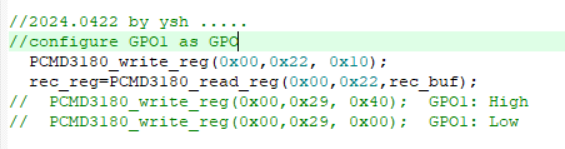
//# Configure PDMCLK1_GPO1 as PDMCLK by I2C write into P0_R34
//w 98 22 41
PCMD3180_write_reg(0x00,0x22, 0x41);
//# Configure PDMCLK1_GPO2 as PDMCLK by I2C write into P0_R35
//w 98 23 41
PCMD3180_write_reg(0x00,0x23, 0x41);
//# Configure PDMCLK1_GPO3 as PDMCLK by I2C write into P0_R36
//w 98 24 41
PCMD3180_write_reg(0x00,0x24, 0x41);
//# Configure PDMCLK1_GPO4 as PDMCLK by I2C write into P0_R37
//w 98 25 41
PCMD3180_write_reg(0x00,0x25, 0x41);
//# Configure PDMDIN1_GPI1 and PDMDIN2_GPI2 as PDMDIN1 and PDMDIN2 by I2C write into P0_R43
//w 98 2B 45
PCMD3180_write_reg(0x00,0x2b, 0x45);
//# Configure PDMDIN3_GPI3 and PDMDIN4_GPI4 as PDMDIN3 and PDMDIN4 by I2C write into P0_R44
//w 98 2C 67
PCMD3180_write_reg(0x00,0x2c, 0x67);
//# Enable Input Ch-1 to Ch-8 by I2C write into P0_R115
//w 98 73 FF
PCMD3180_write_reg(0x00,0x73, 0xff);
//# Enable ASI Output Ch-1 to Ch-8 slots by I2C write into P0_R116
//w 98 74 FF
PCMD3180_write_reg(0x00,0x74, 0xff);
//# Power-up PDM converter and PLL by I2C write into P0_R117
//w 98 75 60
PCMD3180_write_reg(0x00,0x75, 0x60);
After setting the PWR_CFG register, we can read to the correct setting value(0x60).
// # read PWR_CFG Register
rec_reg=PCMD3180_read_reg(0x00,0x75,rec_buf);

Then we read DEV_STS0 and DEV_STS1 register and found the DEV_STS0/ DEV_STS1 value is 0x00 and 0xc0 respectively.
The meaning all PDM channels turned off.

// # read DEV_STS0 Register
rec_reg=PCMD3180_read_reg(0x00,0x76,rec_buf);

// # read DEV_STS1 Register
rec_reg=PCMD3180_read_reg(0x00,0x77,rec_buf);

Finally we found no CLK signal output in the pcmd3180.

How to do next step. Please give us some suggestion for the issue. Thanks a lot.
Best regards,
ShengHua