A related question is a question created from another question. When the related question is created, it will be automatically linked to the original question.
If you have a related question, please click the "Ask a related question" button in the top right corner. The newly created question will be automatically linked to this question.
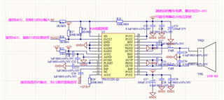
1. the C35 GND connection position should be nearby DAC, and the trace should be matched with INP trace.
2. take care of L1 and L2 inductor's saturation current. it should be larger than 2A
3. C29 and C34 should be larger, typically 1uF or 2.2uF should be used. see datasheet section '8.2.2.5 When to Use an Output Filter for EMI Suppression'