This thread has been locked.
If you have a related question, please click the "Ask a related question" button in the top right corner. The newly created question will be automatically linked to this question.
Tool/software:
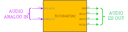
在使用TLV320AIC3262EVM-U的過程中我們有個疑問想請教:就是當我們從TLV320AIC3262的D3和D4 PIN輸入模擬音頻信號時,能不能從TLV320AIC3262的G3/G2/J6/G4 PIN輸出I2S信號?示意如下圖:
Hi,
Yes, you can send analog audio in and get I2S digital audio out. The outputs would be on BCLK2, WCLK2, and DOUT2, not DIN2 since that would be for digital I2S in for use in the DAC. This diagram is describing the device's ADC being used. If you want the clocks to be OUTPUT, you are using the device in "master mode", where you input a master clock, MCLK, and then the device divides it down into the BCLK and WCLKs. If this is not the case, you will need to change the line "w 30 1a 24" to set 1a to 0x00.
The script will change if you have a single ended vs differential input, I included both.
I made the script going off of the examples in the application reference guide (https://www.ti.com/lit/ug/slau309/slau309.pdf) as well as the EVM software's default script examples. Let me know if you have difficulties making it work.
Best,
Mir
################################################################ # ADC Stereo Record - High Performance # SE input signal from IN1L/IN1R # AVDDx_18, HVDD_18, CPVDD_18 = 1.8V; IOVDD, AVDD3_33, RECVDD_33 = 3.3V; SLVDD, SRVDD, SPK_V = 5V, DVdd = 1.8V # MCLK = 12.288, Fs = 48kHz # PLL Disabled, AOSR = 128, PTM_R1 # CM = 0.9V # Primary I2S Interface used with WCLK & BCLK as inputs to the device ################################################################ ################################################################ # Software Reset ################################################################ w 30 00 00 # Initialize to Page 0 w 30 7f 00 # Initialize to Book 0 w 30 01 01 # Initialize the device through software reset d 1 # Delay 1 millisecond ################################################################ # Power and Analog Configuration ################################################################ w 30 00 01 # Select Page 1 w 30 01 00 # Disable weak AVDD to DVDD connection and make analog supplies available w 30 7a 01 # REF charging time = 40ms w 30 79 33 # Set the quick charge of input coupling cap for analog inputs ################################################################ # Clock configuration # MCLK = 12.288 MHz, BCLK = 3.072 MHz, WCLK = 48 kHz (slave) ################################################################ w 30 00 00 # Select Page 0 w 30 04 00 # Set ADC_CLKIN as MCLK1 -- default not mandatory to program w 30 12 81 # Power Up NADC, NADC = 1 w 30 13 82 # Power Up MADC, MADC = 2 w 30 14 80 # Program the OSR of ADC to 128, ADC_FS = ADC_MOD_CLK / AOSR = 6.144MHz / 128 = 48kHz ################################################################ # Audio Serial Interface Routing Configuration - Audio Serial Interface #2 # ASI #2 recording ################################################################ w 30 00 04 # Select Page 4 w 30 11 00 # Audio Serial Interface #2 is set to I2S mode, 16-bit w 30 1a 24 # Route ASI#2 WCLK as output to WCLK2 and BCLK as output to BCLK2 w 30 17 01 # Route ADC data to Audio Serial Interface #2 w 30 18 50 # ASI#2 Left Channel data sent to Left Channel DAC, ASI#2 Right channel data sent to Right Channel DAC w 30 45 04 # Select WCLK2 pin as WCLK for Audio Serial Interface #2 w 30 46 04 # Select BCLK2 pin as BCLK for Audio Serial Interface #2 w 30 47 22 # Select DOUT2 pin as DOUT for Audio Serial Interface #2 w 30 48 20 # Select DIN2 pin as DIN for Audio Serial Interface #2 w 30 76 16 # Only ASI#2 Routed to DAC miniDSP Data Input 1 ################################################################ # Signal Processing Settings ################################################################ w 30 00 00 # Select Page 0 w 30 3d 01 # Set the ADC PRB Mode to PRB_R1 ################################################################ # ADC Input Channel Configuration --- IN1L / IN1R ################################################################ w 30 00 01 # Select Page 1 # IF two SINGLE ENDED INPUTS: w 30 08 00 # Set the input common mode to 0.9V w 30 34 80 # Route IN1L to LEFT ADCPGA with 20K input impedance w 30 36 80 # Route CM1 to left PGA with 20k input impedance w 30 37 80 # Route IN1R to RIGHT ADCPGA with 20K input impedance w 30 39 80 # CM1 to Right PGA M terminal, 20k input impedance # IF DIFFERENTIAL (must be on RIGHT PGA ONLY for IN1) #w 30 37 80 # set IN1R to right PGA P terminal, 20k input impedance #w 30 39 20 # set IN1L to right PGA L terminal, 20k input impedance w 30 3B 00 # Left Channel Analog ADC PGA = 0 dB w 30 3C 00 # Right Channel Analog ADC PGA = 0 dB w 30 3D 00 # ADC Analog programmed for PTM_R4 w 30 00 00 # Select Page 0 w 30 51 C0 # Power-up ADC Channels, left and right w 30 52 00 # Unmute ADC channel and Fine Gain = 0dB
(I machine translated this, sorry for any errors):
您好,
是的,您可以發送類比音訊輸入和接收 I2S 數字音訊輸出。 輸出將在 BCLK2 , WCLK2 和 DOUT2 上,而不是 DIN2 上,因為這將用於 DAC 中的數位 I2S。 此圖說明使用的裝置 ADC。 如果您想要輸出時鐘,您就在「主要模式」下使用裝置,輸入主時鐘 MCLK ,裝置隨後會向下分為 BCLK 和 WCLK。 如果不是這種情況,則需要將“ w 30 1a 24 ”行更改為將 1a 設定為 0x00。
如果您有單端輸入與差動輸入,指令碼將會變更,我同時加入兩者。
我在指令碼中不再列出應用參考指南 (www.ti.com/.../slau309.pdf) 中的範例,以及 EVM 軟體的預設指令碼範例。 如果您在工作中遇到困難,請告訴我。
敬頌教安,
和平號