This thread has been locked.

If you have a related question, please click the "Ask a related question" button in the top right corner. The newly created question will be automatically linked to this question.

PGA2311: Issues with DC offset and Zero Crossing Detection (ZCD)

Part Number: PGA2311
Other Parts Discussed in Thread: OPA1678, PGA4311

Tool/software:

Hello,

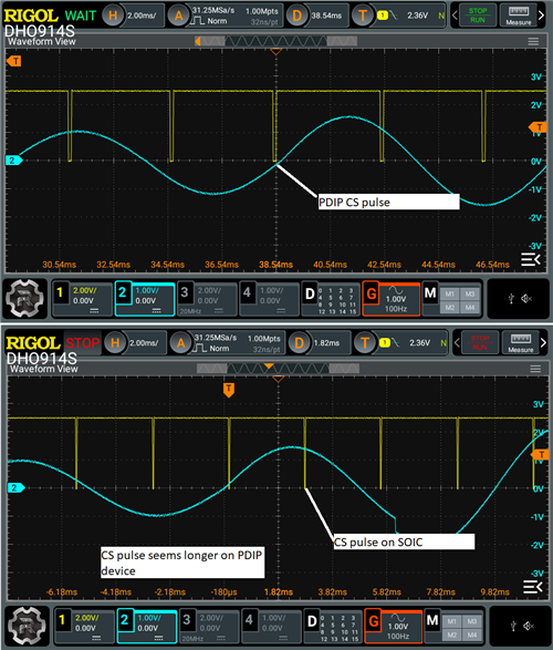
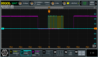
I'm using the PGA2311 in a product for approx. one year and it worked like a charm. No noticeable noise when changing volume. After the first two batches I changed from the PDIP package to the SOIC package and that's when the problems started. All of a sudden there is very noticeable noise when changing volume, especially above 0dB. These has two sources:

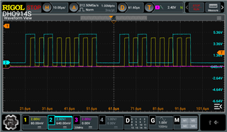
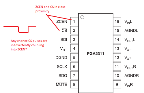
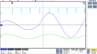
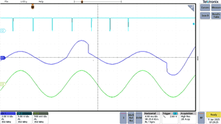
  1. The zero crossing detection started to behave oddly. It seems like the ZCD stops to work, when there are messages sent before the ZCD detects the zero crossing of a previous command. I only could get that under control with a waiting period of 18ms before sending the next message. This is a problem, because I need a very smooth fade and these 18ms waiting periods are noticeable under some circumstances.
    With the PDIP package the ZCD works like there is only a change in volume after a zero crossing or a timeout of 16ms. With the SOIC package there is an immediate change in volume, if the PGA2311 waits for the zero crossing of a previous volume change command and a new volume change command is issued.

  2. The parts with SOIC package had a DC offset. I have a DC blocking capacitor on the input and with that the measured DC offset was up to +-500uV which results in a DC offset of some mV after the gain. This DC offset leads to a very strong swichting noise. To get that under control I had to remove the DC blocking capacitor and hand select opamps of the input stage to get a DC offset of under 100uV which resulted in the volume changes being quiet to up to +20dB. This wasn't the case with the PDIP package. I measured an old one with the PDIP package and it has almost 0uV DC offset.

Is there any information of changes between packages or even batches?

  • Hello Uwe,

    The PGA2311 has not gone through manufacturing device changes. From the device design perspective, there is no difference on the device die between PDIP and SOIC packages. The two packages use the same spec. There are two grades affecting THD+N performance and input capacitance.  The A-grade is the higher performance (PGA2311PA -PDIP, PGA2311UA -SOIC), and U-grade is the standard grade (PGA2311P -PDIP, PGA2311U -SOIC),  but these specifications apply to both PDIP or SOIC packages.

    To help diagnose/debug the issue, please help with the following information:

    1) Kindly submit the full-schematic, and if possible, the PCB layout Gerber plots of both your PDIP and SOIC package design

    2) How many tested SOIC Devices show the unexpected behavior?

    3) What is the voltage of the digital supply VD? What is the voltage on the ZCEN pin on the devices that show the behavior?  

    4) What signal source or circuit is driving the PGA2311? What is the input signal amplitude at the Gain above 0-dB when the issue occurs?

    5) The PGA2311 expected max input offset is right at ±500uV maximum for both packages, and both grades. What gain do you use to measure PGA2311 offset? What procedure is used to measure the offset, are the inputs shorted to measure the offset? and how many devices show an offset around ±500µV?

    Thank you and Kind Regards,

    Luis

  • Hello Luis,

    thanks you for your reply. Both the PDIP and the SOIC were U-grade.

    1. Where can I submit the schematic and layout/gerber files?
    2. Until now 20 out of 20 SOIC devices showed the behaviour. The batches before that with the PDIP devices were 10 and 15.
    3. Supply voltage of VD+ is 5V, ZCEN is tied to VD+.
    4. There is an opamp buffer (OPA1678) with AC coupling capacitor before the PGA2311. The signal amplitude doesn't change the offset. It occurs with very small as well as maximum amplitude. Measurements of the ZCD were done with 1Vpp sine wave.
    5. I measured the input offset with open inputs since the PGA2311 has a 10k input impedance to GND. So this is the offset the PGA2311 would see if AC coupled. The gain didn't change the input offset, only the resulting output offset. All devices showed an offset above the typical 250uV. The max offset were measured by approx quarter to a fifth of the devices.

    I'm aware that 500uV is the maximum input offset according to the data sheet, but the device isn't switching silently with that offset.

  • Hi Uwe,

    Yes, you are correct that the magnitude of the input referred offset is ±500µV max, and the output offset for gains of 0dB and above is VOS*Gain. The PGA2311 zero crossing feature applies gain changes (or mutes) until either a positive slope zero crossing is detected, or a time out occurs, in an attempt to minimize or reduce audible artifacts. If the gain changes are occurring within the inherent input referred offset of the PGA device, and this gain change is still audible on the smooth fade application, unfortunately, this may be within the limitation of the capability of the zero-crossing function of the PGA2311 device.   

    If you wish us to review the schematic and layout,  I can certainly help with this. You may post the schematic and layout files on E2E using the insert button on the menu options below. Alternatively, if you do not wish to post your schematic on E2E, let me know and I can contact you via private conversation to review the schematic.  

    Thank you and Regards,

    Luis

  • Hey Luis,

    sorry for the late reply. I'd rather not post the schematics here, but I also doubt that this is the problem here, because (among other reasons) the layout worked with the PDIP package.

    Anyway, the problem with the input offset renders the device unusable for everyone using it above 0dB. Apparently different batches have wildly different DC offset. The first 20 I had had no measurable DC offset and the following 20 had the explained offset. 500uV are too much to operate the device quietly. DC offstes below 50uV allow to operate the device quietly up to 18dB.

    And that doesn't explain the issues with the ZCD. I'm going to try to capture some scope traces that show the behaviour of both old and new chips. But that will take me a while. Please keep that thread open.

  • Hi Uwe,

    Sorry you are experiencing issues. I can look into the ZCD functionality, reproduce the setup on the bench, help debug, and investigate if this is expected behavior or another issue. Regarding the offset, unfortunately, the data sheet only provides assurances for offsets to ±500µV max. You don't have to post the schematic on E2E, but I will follow-up and contact you via private conversation so you may share the information. The schematics, oscilloscope plot and detailed test conditions will help us measure the behavior/debug/reproduce the issue. 

    Thank you and Kind Regards,

    Luis

  • Hey Luis,

    here are some scope traces. For all traces Channel 1 (yellow) is the Chip Select of the SPI communication. Channel 2 (blue) is the output of the PGA2311. It is fed with a 100Hz 1Vpp sine wave.


    These two images are from the SOIC package. With only a single command the zero crossing detection works as expected.


    These two images are from the exact same device with exact same measurement conditions, but with repeating messages sent. These repeating messages contain a volume sweep. Every pulse on channel 1 is one message of the sweep sent. You can clearly see, that the zero crossing detection doesn't work all the time.


    And finally, these two images are from the PDIP package. This PGA2311 I just ordered from Digikey. The zero crossing detection works as expected with multiple messages sent.

    When listening to the output of the sweep of both packages it's like the waveforms suggest. The PDIP package is abolutely smooth, whereas the SOIC package is full of crackles.

  • Hi Uwe,

    Can you please include a zoom in oscilloscope plot of the CS, SDI, SDO, SCLK on both the PGA2311P and PGA2311U? I would like to verify the serial interface timing on the command sequence.

    Is there any difference in timing between the two PDIP and SOIC solutions?  At first sight, on the scope shots above, the CS pulses appear to be much wider on the PDIP package when compared to the SOIC oscilloscope plots.

    I have a sample order for fresh PGA2311U devices that should arrive later this week to perform testing; the units that I currently have in hand do not show any anomaly.

    Thank you and Best Regards,

    Luis

  • Hey Luis,

    here is the timing of the SOIC package. CS in purple, SCK in yellow, SDI in blue.


    This is the timing of the PDIP package.

    The timing is a bit different. The PDIP uses another micrcontroller without a FIFO, so there is a little break between the bytes. PDIP is also a bit slower, but as far as I see both are well within the timing constraints of the datasheet.

  • Hi Uwe,

    • I have reviewed the timing on the SPI interface oscilloscope plots above for SOIC/PDIP; and specs are met. SDI is changing state on the SCLK falling edge and read on SCLK rising edge.  On SOIC, SCLK frequency is about 1 MHz which is well within spec. tSDS, tSDH, tCSCR, tCFCS specs are met. No obvious issue on the SPI sequence on SOIC or PDIP
    • I have not been able to reproduce an immediate issue with the PGA2311 devices at hand. Nevertheless, I plan to spend additional time later this week and attempt to duplicate the timing on SOIC as close as possible (within the limitations of the SPI driver used on my setup). I am still waiting for new/fresh PGA2311 SOIC devices. I expect to receive within the next 2 business days; and perform additional tests by the end of this week.
    • From the PGA2311 manufacturing perspective, the PDIP and SOIC devices use the same device die and same test program sequence. It is difficult to explain why would they behave differently. We have no reported cases of PGA2311 failures at this point
    • I have not yet reviewed your schematic and PCB layout, since you have mentioned that you don’t believe the issue is related to the schematic. If you wish me to review the schematic and PCB layout, you can certainly submit these documents on the private conversation thread.

    If you believe the SOIC devices are defective or failing devices, you may start the process for Failure analysis through TI Customer quality.  The team may request the schematic submission as part of the documentation.

    Please find a few links with pertinent information.

    Failure analysis

    Contact TI customer quality via CPR (customer product return)

    Follow TI's guidelines for handling customer returns

    I will update once I receive and test the fresh SOIC sample devices by Friday evening or Monday morning US time.

    Thank you and Regards,

    Luis

  • HI Uwe,

    If possible, one quick check/question regarding the PGA2311 SOIC solution, 

    Is the ZCEN driven high with a GPIO or pull-up resistor? Or is this permanently connected to the VD+ supply?

    Can you kindly verify/check with the oscilloscope for low voltage transients/glitches on the ZCEN pin by placing the oscilloscope probe right on the ZCEN pin? 

    On the oscilloscope plots on the post above, the unexpected non-zero crossing gain changes always occur somewhat randomly, but always shortly after the CS pulse after what appears to be a constant delay.  Since the CS pin is in very close proximity to the ZCEN pin, any possibility that the CS pulse signal (or perhaps any other external noise signal source) is coupling into the ZCEN pin producing a glitch on the ZCEN voltage?

    Thank you and Kind Regards,

    Luis 

  • HI Uwe,

    Some quick tests on the units do not appear to show anomalies as far.  See below. 

    Although, my SPI driver does not use the exact same timing.

    An oscilloscope capture of the PGA2311 VOUTR output and CS is below.

    Thank you and Kind Regards,

    Luis

  • Hey Luis,

    good point with the CS coupling into ZCEN. I checked, but not a tiny bit of coupling measurable. It is pulled up to 5V with a 2k2.

    About your measurements: I only see the first message on the trace. The problem only appears though, when a second message is sent, before the first zero crossing.

    I have five of the problematic chips left. Would it be of help, if I send one over to you?

  • HI Uwe,

    Happy New Year!  I was out of office for the last couple of weeks during the Holidays, therefore the delayed response.

    Kindly allow me a couple of days to get a hold of a different digital card that allows better control and flexibility in the timing for these tests.  The goal would be to test / reproduce the timing you use for the SOIC device. I will perform more tests in the next couple of days and provide an update.

    Thank you,

    Kind Regards,

    Luis Chioye 

  • Sure, take your time. It's not a pressing matter. I ordered some PDIP units that seem to work. So I'm set for the next couple of months.

  • Hey Luis,

    there are some interesting developments here:

    Like I said, I ordered some PDIP units and they have very small DC offset as the others, so no problems here. But the thing with the zero crossing deteciton is the same than with the SOIC units. So, I guess it's not the chip.

    To find out if the problem is the software or the hardware, I build the parts of the circuit (the micrcontroller and the PGA2311) on a breadboard and it worked. To find out what part of the circuit is causing problems I swapped the power supplies and signals on the breadboard with supplies and signals from the hardware, one by one. In the end all signals and supplies came from the hardware and it continued working. So, it must be the hardware.

    Next I tried to find out what parts of the hardware are causing the problems and it seems like it's the SPI signals. When I wire these off board, it works. I also found out, that I can get it to work if I attach a long wire to one of the SPI signals with nothing on the other end. I also can get it to work when simply touching one of the SPI pins.

    I started to fool around with resistors and capacitors but no luck. I tried resistors of different sizes to GND, capacitors with different sizes to GND. I tried series resistors of different sizes and added capacitors to GND to it. Nothing seems to work.

    I also found out, that there is a time pattern. I recorded a video of the scope. Here I trigger on a certain message. It looks like the part, when the zero crossing detection is not working, is always at the same message. But it's not the message, it's the time distance between the last time when there was a break in the constant stream of messages. It then continues in steps of 19ms. Every 19ms the zero crossing detection is not working, only when there was a break in the stream of messages longer than 19ms. 

    I'm out of ideas here.

  • Hi Uwe,

    Last week, I performed a number of tests on PGA2311 SOIC, and PDIP package units from different lots, as well as the PGA4311.

    I was able to reproduce timing circumstances, across all devices, regardless of package, or production lot, where the zero-crossing detection did not work reliably. Depending on the delay between the SPI PGA gain control commands, I was able to reproduce conditions where the zero-crossover function did not work properly.  This occurred on most units I tested, regardless of package, or production lot.

    For example, in the testing of the PGA2311 device below, the PGA Gain control commands are issued about 4 milliseconds apart from each other. In this particular case, with this particular test, the device appeared to work properly:

    However, same device, tested again a couple of days later, if I varied the timing between PGA gain control commands slightly, while still keeping the SPI command timing structure the same, in some cases, I was able to capture cases where the zero crossing was not working reliably.  See below:


    During last week testing on samples from different packages (PGA2311 SOIC, PDIP, and PGA4311 devices), the zero-crossing function worked reliably, when the PGA gain change commands were separated by a delay that exceeded the timeout of 16ms.  In other words, if the micro controller issues the PGA gain change commands separated by a delay longer than the time out, for example 25ms, allowing the previous PGA gain change command to execute, the zero crossing function worked without issue. The behavior was present on the different samples tested, regardless of package or lot, and therefore, the issue is not likely related to package, or production lot. 

    To the best of my knowledge, the behavior has not been reported before. I will discuss with the team, and see if we can document on the data sheet that the zero crossing function requires allowing a longer delay than the time out between gain change commands. The PGA2311 was introduced to the market on 2001, 23 years ago, therefore, additional engineering information about the internal digital state machine is limited.

    Thank you and Best Regards,

    Luis

  • Hey Luis,

    thanks for getting further into that. That is a surprising development. First, I changed the topic of the thread to "Issues with DC offset and Zero Crossing Detection (ZCD)", so it's easier to find for other folks.

    Have you read my previous post? I came to the same conclusion, that package and/or batch is not the issue. For me it seems like the zero crossing detection is thrown off, when commands are received while waiting for a zero crossing. But, like you also stated, not every time!

    Curious how this develops.

  • Hi Uwe,

    Yes, I discussed the same behavior with the engineering team previously; and I will propose to the team to add a note of this behavior on the data sheet. On my tests, the zero crossover function was reliable across all devices while allowing the previous PGA gain change command to execute, ie, allowing a delay longer than the >16ms timeout by some margin.  For example, the PGA zero crossover function was reliable while allowing a delay of 25ms between PGA gain change commands.

    Thank you and Best Regards,

    Luis

  • Thank you for confirming my inital post.

    There are a few questions left. There are some situations where the error occurs and some where it works reliable, regardless of the time between messages.

    • Why does the ZCD work reliably with some PCB designs and doesn't work with others? (It worked reliably with my old design, but doesn't work at all with the new design)
    • Why does it work reliably on a breadboard?
    • Why does it start working when I attach a long wire to one of the pins of the serial connection.
  • Hi Uwe,

    The tests performed on previous weeks while testing different samples (as well as today's measurements) confirm a very consistent result where the zero-crossing works reliably when the PGA gain change commands are issued with a delay longer than 25ms, or essentially allowing the previous gain command to execute AND/OR allowing the 16ms (+ additional delay for margin) timeout to expire. 

    Based on these tests, one can conclude that the logic control was validated allowing a delay for the command to execute, as this function is reliable when allowing the long delay between commands. It appears that the digital control may not be designed to receive multiple gain change commands without allowing the previous gain change command to execute, since this result is consistent among all the devices.

    Using slower/faster SCLK frequencies, and two different digital set ups, with slightly different SPI wire lengths on the interface connections did not appear to change the intermittent results when not allowing the long delay within commands; on my side, the different test results appeared to be more related to the instant where the command is received with respect to an internal logic timing event; and the failure was somewhat intermittent with most sequences, but likely related to the delay changes between commands. The digital SPI interface signals on my test set up were clean and did not have any excessive ringing, nor any violation on the interface timing. Read and Write transactions were always reliable/successful. 

    When reviewing the legacy design engineering documentation, the available information is primarily focused on the analog circuitry; and information of the digital control block is generic / limited. Unfortunately, the main design engineer (and design team) is no longer with TI, since this is a relatively old device from 2001 (PGA2311) 2002 (PGA4311). Without in depth information on the logic control detail, the only recommendation, based on all these tests, is to allow a delay much longer than the timeout for a reliable result. 

    Thank you and Regards,

    Luis

  • I assume not much more will happen here regarding this issue. Sad, because I saw it working and I'm sure there is something that can be done about it. Anyway, for me it's switching to another design and another part because with the waiting time it's too slow and it is not a smooth transition anymore.