This thread has been locked.

If you have a related question, please click the "Ask a related question" button in the top right corner. The newly created question will be automatically linked to this question.

LME49830

Hi,

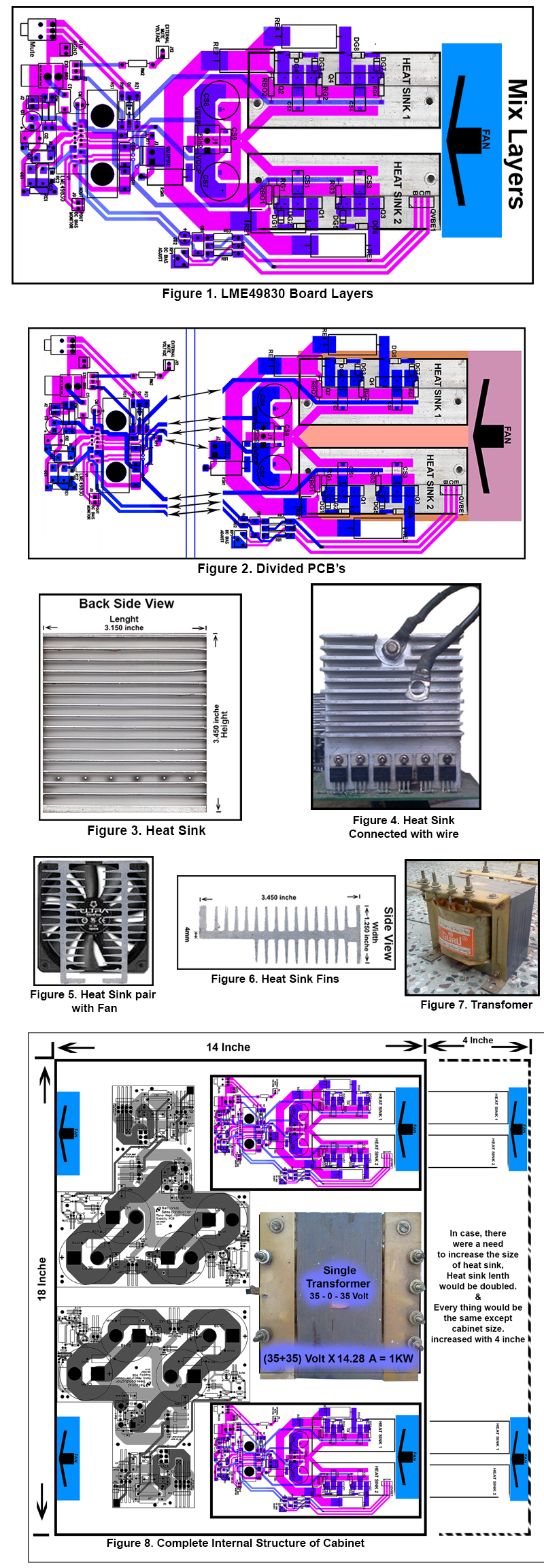
I am working on stereo amp based on LME49830. For it I am following the Reference Designs given in PDF files snaa057a & snaa058a completely. I live in Delhi (India). Where getting the branded components is very hard, which is creating the need to compromise with components values and brands. So my quarry will be based on changed brands and values.

Please don’t mind, if I keep asking questions or silly questions. :(

1Q. is it possible to use (Q VBE1) TIP31C Instead of BD139? If yes, what changes would be required?

(Note- I saw in data sheets, transistor leads positions are different)

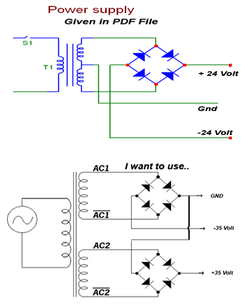
2Q. is it possible to use single primary & dual secondary (35V, 500VA per secondary coil) in Transformer instead of using 4 transformers 24V, 300VA for stereo? If yes what changes would be required?

(Note- I want to use double Power Supply for stereo but with single transformer)

3Q. Using dual rectifier instead of single rectifier, Will it be benefited?

(Note- in PDF file snaa057a, single rectifier with torrid transformer is used, but  I want to use dual rectifier with dual secondary transformer.)


 Thanks For your support.

 Regards

Pankaj Kumar

  • Hello Pankaj Kumar,

    Yes you can use TIP31C as VBE multiplier without any changes in the specified circuit, this transistor fixes the output devices bias voltage and sets the quiscent drain or collector current.

    And yes you can use a single primary toroidal transformer with two secondries I will do the same.

    I think that's better to use only one bridge rectifier with an adequate heatsink. Connecting the two secondaries in series as in the datasheet of the transformer and you'll have the gnd (common) point.

    Thank you very much for your atention,

    Best regards,

    Daniel Almeida

  • Sorry to intervent the discussion, however I have had  bad experience using low gain transistors in VBE circuits. If the internal gain in this contant voltage circuit is not high enough, the bias voltage will change as function of the current through this bias circuit. An excellent paper about this topic is presented by Hawksford, called "Optimization of teh amplified diode bias circuit for audio amplifiers". It can be found on the web.

    In the past I have designed mosfet amplifiers using BD139 as bias sensing transistor, in however during large scale production it turned out that we could only use the devices with really high Hfe ( >250) in order to get consistant performance over the specified temperature range. There are a lot of power transistors on the market ( like TIP series) that are produced by many different manufacturers, even using different diffusing processes. I have seen transistors that had very low Hfe at low collector current, rising to a " maximum" value at 1amp and falling down again at high collector current.

    One other question about LME demoboard to Texas: In the snaa058b, article about reference design, I miss the performance graphs.  Chapter7 has only the header, followed by the board layer views...

    regards

    Geert de Vries

  • Hi

    First of all I want to say thanks to Greet de Vries for giving his valuable suggestions.

    I have been still working on same project of LME49830. I have some questions; I know TI Team will suggest me best.

    I am giving you my whole plan, please verify it.

    My Questions

    Q. 1- Is my modified LME49830 PCB correct as shown in Figure 1?

    Q. 2- Is it possible to divide PCB into two part connected with two connectors (7 Pins). If yes, is there any need to add any extra components? Will dividing PCB increase any distortion in sound? Please have a look at figure 2.

    Q. 3- Is the heat sink size perfect? Or I have to increase its length as I can do this easily however it will also increase the size of cabinet. Have a look on figure 3, 5 & 6.

    Q. 4- Is it possible to connect VCC wire & VEE wire directly to heat sink 1 & 2? See Figure 4.  To make it more stable PCB. If Yes, Will it make any decrease in sound performance?

    Q. 5- How would I connect two power supply board with one Transformer? See figure 8.

    Q. 6- Is the position of all PCB's & transformer correct as given in first figure 8?

    Regards

    Pankaj Kumar

  • Hi, Pankaj,

    This is a specialized device, and unfortunately, the guy who knows about it has left TI, so we are unable to comment further beyond what is published on our website.

    -d2

  • Hi, Don Dapkus,

    Thanks for reply.

    I am really sad to hear this, that the guy who knows about it has left TI. But company does not rely only on one person.

    However I have seen lot of engineers answering questions based on LME49830 on TI website.

    Even I have seen your answers based on LME49830.

    So saying this, there is nobody in TI company who can give answers based on LME49830, will not be true.

    Yes, if you don’t have time to answer to my small questions, may be silly questions that will be fine to write.

    Regards

    Pankaj Kumar

  • Hi,


    I had a quick look at your design. What output devices are you using?

    In general, you should avoid long traces to mosfet gates. Also the source resistors should be non-inductive types.

    In your design, traces to the gates are quite long, and  the source resistors -judging from the shape- are leaded wirewound types.  In combination with the very high openloop gain of the LME and the non-lineair gate capacitance of the fets this is an open invitation to severe HF oscillation of the output stages.

    For the source resistors, be shure to use non-inductive ( in fact really nothing is "non-inductive") low-inductive resistors. We use 4 or 5 thick film 1W smt resistors in parallel with goor results. Make traces between LME and gates as short as possible. Also traces to the temp sense transistor should be short. Keeping output feedback trace, gate driver traces and traces tot temp sensor short and  close together, this minimises stray capacitance, also because they all have the same ac signal. Best practice is to have the LME close to the mosfets ( < 1inch) or have the LME on the centre of the heatsink and the powermostfets located left and right next to the LME.

    success Geert