Because of the Thanksgiving holiday in the U.S., TI E2E™ design support forum responses may be delayed from November 25 through December 2. Thank you for your patience.

This thread has been locked.

If you have a related question, please click the "Ask a related question" button in the top right corner. The newly created question will be automatically linked to this question.

Asymmetrical output bias on TPA6100

Other Parts Discussed in Thread: TPA6100A2

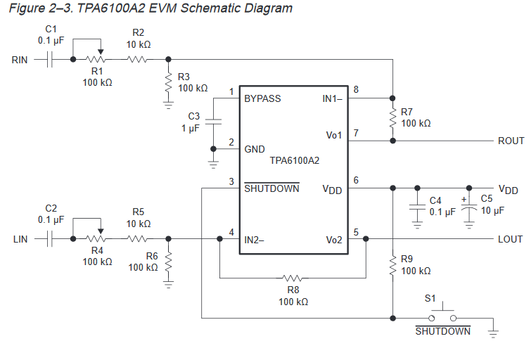
I've built up the TPA6100A2 EVM circuit for myself on a breadboard:

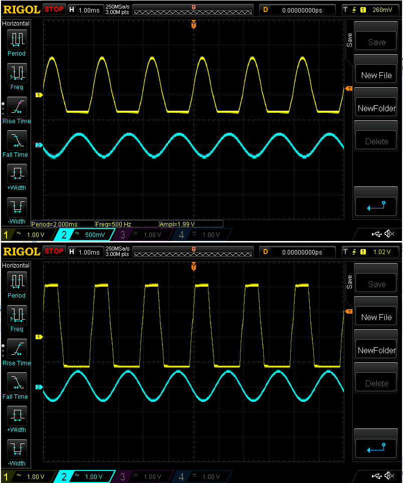
Unfortunately I can't understand why I am getting asymmetrical clipping on the negative side of the amplified signal. In the captures below the yellow trace is the AC coupled output at ROUT and the blue trace is the input sine wave at 500Hz. On the bottom picture the input was turned up on purpose to overdrive the TPA6100 and more clearly demonstrate the asymmetrical clipping. Is this normal for this opamp? Otherwise, how may one go about correcting this behavior?

The resistors on my circuit are 5% through hole so I understand there could be variability from that but I took care to closely match R3 to R7 and R6 to R8.

Thank you,

-Marco

  • Hi Marco,

    Welcome to e2e!
    Are you using the same values for every component on the EVM schematic?
    Are you using AC coupling on the oscilloscope? Could you measure the input signal at IN1-/IN2- pins withouth coupling? Just to make sure that the input signal is properly centered to 0-V.
    What is the voltage at the bypass pin?

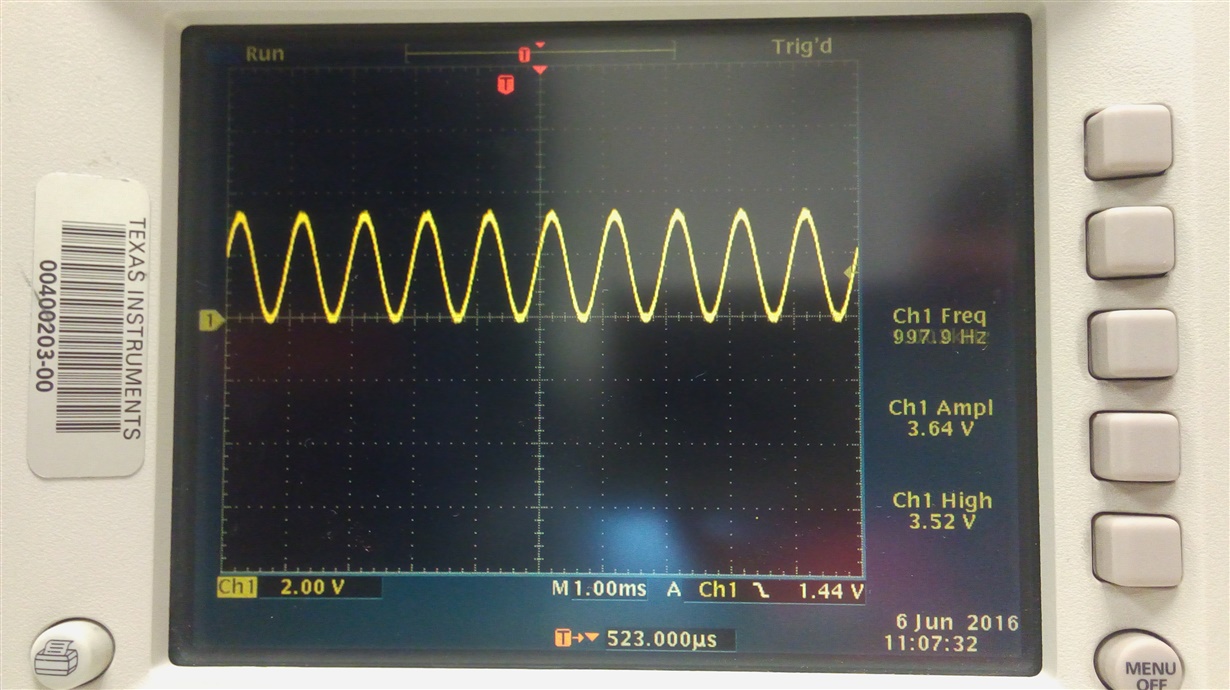
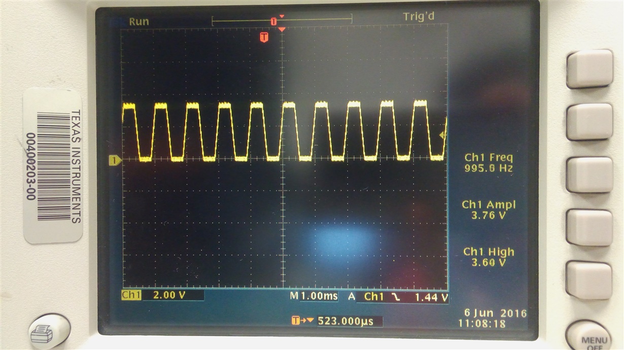
    The output of the TPA6100A2 should clip symmetrically. The following figures were captured using an EVM.


    Best regards,
    -Ivan Salazar
    Texas Instruments

  • Hi Ivan,

    Sorry for the late reply, I finally got a chance to follow up on this circuit. I double checked the setup of my circuit against the EVM schematic. There is no difference in the values used for the components except that on the output I have 100uF coupling capacitors for the output. I also replaced the 1uF bypass capacitor I used at the beginning with a 10uF to see if maybe the bias resistors needed more stability but it did not seem to help too much. The supply is a bench power supply at 3.3 volts with plenty of capacity to drive the circuit.

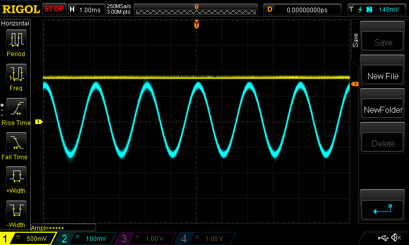
    Here is a picture of the input signal (channel 2 - blue) and the voltage at IN2-. I checked the voltage at IN1- and it is the same. Both channel 1 and channel 2 are DC coupled. The voltage at IN2- is about VDD/4 instead of VDD/2

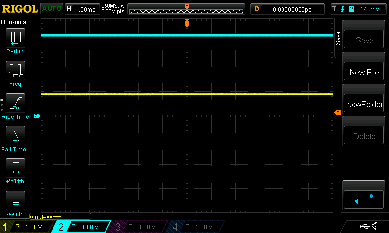
    Here is a picture of the voltage at the bypass pin (channel 1 - yellow) and the VDD pin (channel 2):

    I will add that I put together the circuit on a breadboard with through-hole components and the TPA6100 mounted on a small breakout. My circuit is not using SMD components on a PCB. However, the signals are pretty clean considering my work environment and the breadboard so I am not sure this is the cause of the problem, just thought it would be good information to provide you.

    Thanks!

    -Marco