This thread has been locked.

If you have a related question, please click the "Ask a related question" button in the top right corner. The newly created question will be automatically linked to this question.

TLV320ADC3101IRGE

Other Parts Discussed in Thread: TLV320ADC3101

Hi 

I am using this chip for connecting to a TX1 module from nvidia 

The chip is connected to the processor through the I2S and I2C interfaces 

I am able to write the configuration to the Device configured in I2S slave mode 

I have given BCLK MCLK and WCLK for the chip from the processor 

BCLK----------2.822 MHZ

MCLK----------11.286MHZ

WCLK----------44.1KHZ

In the reference board the chip is configured in I2S slave mode 

we are getting the same values of clock from the micro controller  in reference board 

But we are not able to find any activity in our board in Dout Pin. whereas in reference board there is activity in the Dout pin 

What are the possible checks can be done for debugging this 

  • Hello,

    In order to ensure that the TLV320ADC3101 will start sending data through the DOUT Pin, it is necessary to verify the following settings:

    - Power supplies enabled and stable. Please verify that all the power supplies respect the recommended operating conditions of datasheet.
    - WCLK and BCLK in phase.
    - PGA and ADC un-muted and enabled.
    - Clock PLL/dividers enabled. It is necessary to ensure that the sampling rate is being configured correctly. Once the clock dividers (and PLL if used) are enabled, you should get an output signal at the DOUT pin.

    Best regards,
    Luis Fernando Rodríguez S.
  • hi we are facing the same issue in one of our boards again 

    AGC is set as zero automatically in this board 

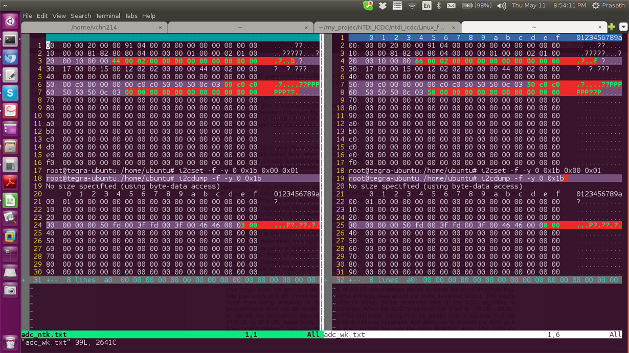
    I2C link is working fine the following is the register dump comparison of working and not working boards

    what else can be the cause 


  • Hi,

    I would recommend to take a look at the following registers configuration. It contains the minimal registers that must be configured in order to have the ADC3101 fully operating. The registers are in hex format: w (write) 30 (I2C address) xx (register address) yy (register data) zz (next register data).

    ###############################################
    # Software Reset
    ###############################################
    #
    # Select Page 0
    w 30 00 00
    #
    # Initialize the device through software reset
    w 30 01 01
    #
    ###############################################


    ###############################################
    # Clock Settings
    # ---------------------------------------------
    # The codec receives: MCLK = 11.2896 MHz,
    # BLCK = 2.8224 MHz, WCLK = 44.1 kHz
    ###############################################
    #
    # Select Page 0
    w 30 00 00
    #
    # NADC = 1, MADC = 2
    w 30 12 81 82
    #
    # AOSR = 128 (default)
    #
    ###############################################

    ###############################################
    # Audio Settings
    ###############################################
    #
    # Default Setting: I2S, 16-bits, Slave Mode (BCLK and WCLK are inputs), 3-stating of DOUT disabled
    w 30 1b 00
    ###############################################
    # Signal Processing Settings
    ###############################################
    #
    # Select Page 0
    w 30 00 00
    #
    # Set the ADC Mode to PRB_P1 (default)
    w 30 3d 01
    #
    ###############################################


    ###############################################
    # Recording Setup
    ###############################################
    #
    # Select Page 1
    w 30 00 01
    #
    # Select MICBIAS1 = MICBIAS2 = 2.5V
    w 30 33 50
    #
    # Left ADC Input selection for Left PGA = IN1L(P) as Single-Ended
    w 30 34 fc
    #
    # Right ADC Input selection for Right PGA = IN1R(M) as Single-Ended
    w 30 37 fc
    #
    # Left Analog PGA Seeting = +25dB
    w 30 3b 32
    #
    # Right Analog PGA Seeting = +25dB
    w 30 3c 32
    #
    # Select Page 0
    w 30 00 00
    #
    # Power-up Left ADC and Right ADC
    w 30 51 c2
    #
    # Unmute Left and Right ADC Channels (Gain = 0dB)
    w 30 52 00
    ###############################################

    Best regards,
    Luis Fernando Rodríguez S.
  • Hi Luis Fernando Rodríguez S.

    We have checked this and we have set this configuration through driver 
    but still we are facing the same is there any thing at the pin level can be checked if the ic is fully functional  

  • Hi,

    I would recommend to follow the next steps for debugging:

    - Verify that the audio ADC is receiving the I2S clocks. The DOUT pin cannot generate any data stream if the device is not getting the correct clocks values. Additionally, ensure that the I2S timing is respected ( www.ti.com/.../slas553b.pdf ).
    - Then, verify that the I2C lines are working correctly. Specially, verify that the I2C address is correct.
    - Finally, if the ADC3101 is correctly configured, you should get a common-mode voltage at the analog inputs. It should be around 1.35V.

    Please let me know if you get some observations about the ADC behavior.

    Best regards,
    Luis Fernando Rodríguez S.
  • Hi Luis Fernando Rodríguez S

    we have probed the I2S lines B CLK INPUT TO ADC is it 256khz W CLK INPUT TO ADC is 8khz

    and we have taken I2C dump and captured the register values so i think I2C is working fine 

    we are able to read the registers from the device so no issues in this 

    and out of 20 board s only in 5 we are facing this problem 

    thatch why we are not suspecting any th


  • Hi,

    Could you provide details about the analog input pins (IN1L and IN1R)? What is the voltage level at these pins before and after the registers configuration? Additionally, are you using a MCLK signal? The registers are configured to generate the sampling rate from the MCLK.

    Best regards,
    Luis Fernando Rodríguez S.