This thread has been locked.

If you have a related question, please click the "Ask a related question" button in the top right corner. The newly created question will be automatically linked to this question.

PGA2320 cascaded delays after 16 shifts

Other Parts Discussed in Thread: PGA2320, SN74AHC594

Hi,

I have a PGA2320 followed by two SN74AHC594 , giving a  32 bit chain: SDI-PGA-SDO-> ser 1st 594 -> QH' -> ser 2nd 594->QH'

I control the chain with a MSP430 SPI (SIMO, SOMI, CLK) and bit bang the /CS pin to load the serial data into the PGA and the 594 output registers after 32 bits have been shifted out in 4x 8 bit by the SPI SIMO and SPICLK. The QH' output of the last 594 feeds back into the MSP430 SOMI pin.

The SPICLK generates a total of 32 clock cycles, clocking data out at the negative edge, that is clocked in the PGA and the 594's at the positive edge.

Serial data is clocked back in the MSP430 SOMI pin on the rising edge of the SPI CLK.

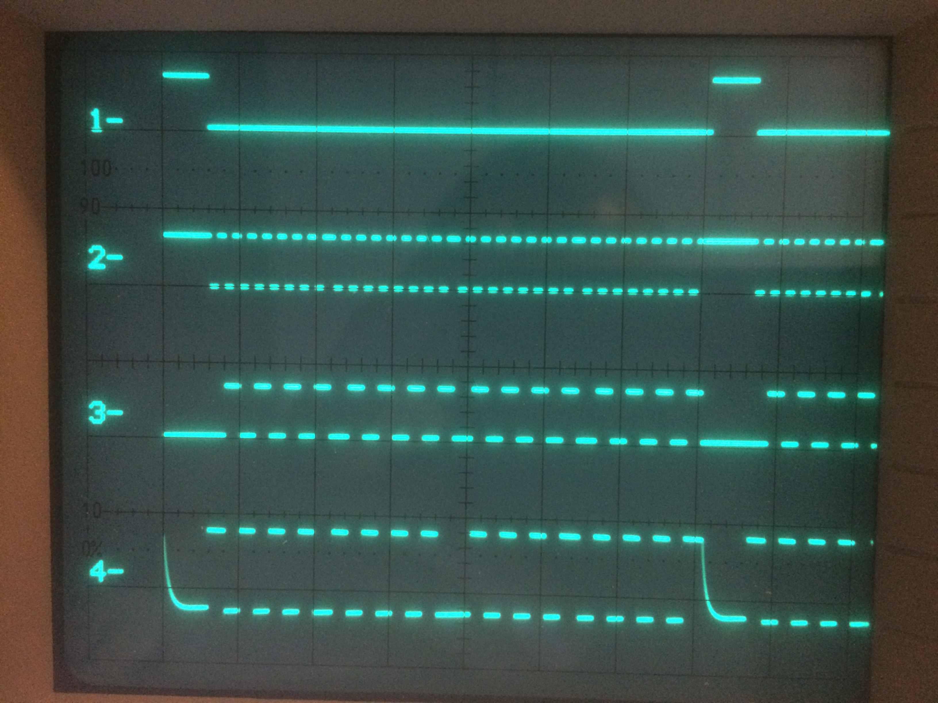
The first 2 bytes read back correctly but the last two bytes are delayed with 1 bit position, so 0X55 55 55 55 clocked in reads out thenext time

as 0X55 55 AA AA.

The PGA SDO output  is delaying the data output 1 bit after 16 clock cycles, causing this one bit shift

I see also the delayed bit coming out of the PGA after 16 clock cycles.

Any idea what can cause this?

I did not have a 100K pull down resistor at the SDO, as indicated in the PGA2320 datasheet (page 10) and found out this pin floats when /CS=high but adding the resistor makes no difference. I would be surprised if it did since the first 16 bits shift out correctly.

The reset pin becomes active high +/-200mS after the powersupply is up.

I checked the minimum VinH (2V) of the PGA which is OK for a 3V3 GPIO from the MSP430.

Also setup and hold times are way within spec since I am driving with a 100KHz clock signal. 

ANy idea what causes this bit delay after 16 clock cycles?

  • Hello Jan,


    You are right to assume that the delay is causing the one bit shift that you are seeing. Since the control data is provided as a 16-bit word and your first 16-bits are coming out correctly, I can assume your serial data for the first 16-bit word is sent correctly.

    However, one can see that the next 16-bit word is truncated—because of this delay—which is why you see 0x55 turn into 0xAA. In other words, 0101 0101 sent, delay occurs even though the first bit 0 has already been sent, and PGA sees 1010 1010.

    When you send the second set of 16-bits, are you setting /CS from low to high and then to low again?

    If so you may not be accounting for the delay it takes for SCLK to start up after /CS goes low and the delay it takes for SDO to output valid data in the form of tCSCR and tCFDO. These delays are tabulated in the datasheet and shown visually in Figure 3 of the datasheet of the PGA2320.

    If you are not please feel free to provide more information about your timing, use of /CS, and other information or waveforms that you think might have missed in your original post to help solve the problem.


    -Cole

  • Cole,

    I have programmed the SPI of the MSP430 as such that first /CS is pulled low, then the first byte is sent, wait for the SPI busy flag to clear, read first received byte from the SPI receive register, then the second byte is sent, wait for SPI busy flag to clear, read second byte received and so on.  After the last byte is read back the /CS line is pulled high again.

    On the scope I see data , clock and /CS going into the PGA2320 /CS goes down, CLK pulsing 32 times, data alternate ones and zero's on negative clock edges and at the end /CS going high again.  As expected.

    If I look then at the output of the PGA2320 I see the data coming out on the negative clock edge, as expected but on the 17th. clock edge the data is stretched by one clock cycle.

    I found an error in my design in that the data is clocked in the PGA2320 from the MSP430 at 3V3 logic level.  That is OK for the PGA2320 but the output of the PGA2320 is at 5V logic level.  The SN74AHC594 that receives the 5Vlevel SDO from the PGA2320 is not 5V compliant. I have to replace that with a SN74LV549. 

    Nevertheless is it strange that only at the 17th. clock pulse, ( /CS stays low), the SDO data gets stretched by one clock cycle.

    As said, I do not have problems with setup and hold times and the CLK is 100KHz.

    One thing to notice is that I have not connected the +/-15V supplies since my powersupply is not ready yet. I have 3V3 and 5V connected to the board using lab powersupplies.

    Is there a dependency of the logic circuits and the analog supply?  My argumentation was sofar that if this would be the case the SDO should be erroneous at all clocks, not only the 17th. 

  • Hello Jan,

    First, I would like to apologize for the untimely response. I have explained your problem to another member of the team and I am still waiting on a reply.

    In the meantime, I revisited your problem and datasheet and I have to ask, is the ZCEN pin low or high? If ZCEN is high then zero crossing detection is enabled. The section outlined in the datasheet explains that ZCEN changes the "gain settings on a zero crossing of the input signal... The new gain setting will not be latched until either two zero crossings are detected, or a timeout period of 16ms has elapsed without detecting two zero crossings."

    Since your analog supply voltage is not ready yet I imagine you left the inputs floating (or not tied to a known voltage) and the ZCEN can't find any valid zero crossings which result in a delay until the new gain setting is latched. Since gain settings come in 16-bit words, this might explain why you see a delay on the 17th bit. Flipping ZCEN to low might solve your problem.

    If your ZCEN is already tied to low then I will update my team member and update you with his response.

    Best,

    -Cole

  • Cole,

    I finished the powersupply PCB earlier this week , no time sofar to test it

    The ZCEN pin is high in my design but it sounds strange to me if the serial chain output gets stalled by the zero crossing detection circuitry.

    You can run the CLK at 6.25MHz, meaning a minimum 16 bit gain update of give or take 16x160nS=2.6uS. The maximum zero crossing timeout time is 16ms. This would mean you mis complete data slots if the ZCEN pin would stall the SDO stream.I assumed the volume data is latched on the low to high edge of the /CS pin and the actual update -> changing the gain setting is only effectuated after the zero crossing or after a timeout. This should not interfere with data clocking through the serial chain, thereby impacting data in other devices further down the chain.

    I'll do the retest once I have the powersupply validated and hooked up.

    Keep you posted.

  • Cole,

    The powersupply is finished and I measured the signals coming from the PGA2320 again with the analog supplies active. The signals are exactly the same with and without the +/-15V supplies.

    I also finished the MSP430 programming. The PGA2320 and two 8 bit shift registers that are in cascade after the PGA are loaded correctly.

    Only the read back of the two last bytes is shifted by 1 bit.

    Attached some scope plots that show on trace 1 the CS, trace2 is CLK (you can see 4 groups of 8 clock cycles with a slightly longer clock time on the start of each next byte clock due to the SPI reload.

    Trace 3 is the SPI data input after the second shift register (4 times code ox55) and trace 4 is the direct output of  the PGA2320

    Picture below that is the enlarged version after 16 clock cycles