This thread has been locked.

If you have a related question, please click the "Ask a related question" button in the top right corner. The newly created question will be automatically linked to this question.

SRC4193: Bypass Mode

Part Number: SRC4193
Other Parts Discussed in Thread: SRC4392

Hi

Do you think that the SRC4193 could transfer DSD audio data in Bypass Mode? In datasheet is refered:

A bypass mode is included, which allows audio data to be passed directly from the input port to the output port, bypassing the ASRC function. The bypass option is useful for passing through encoded or compressed audio data, or nonaudio control or status data.


From what i understand, there is not restriction as for the data format. If PCM data can be bypassed, then and DoP (DSD over PCM) formated could be bypassed. Is there someone having experience on this issue?

Thanks 

  • Hi, Fotios,

    I think your assumption is correct, as long as input and output port clocks are synchronous, this is a requirement for Bypass mode. 

    I have notified a colleague who could provide further comments about this.

    Best Regards,

      -Diego Meléndez López
       Audio Applications Engineer

  • Many thanks Diego for the reply

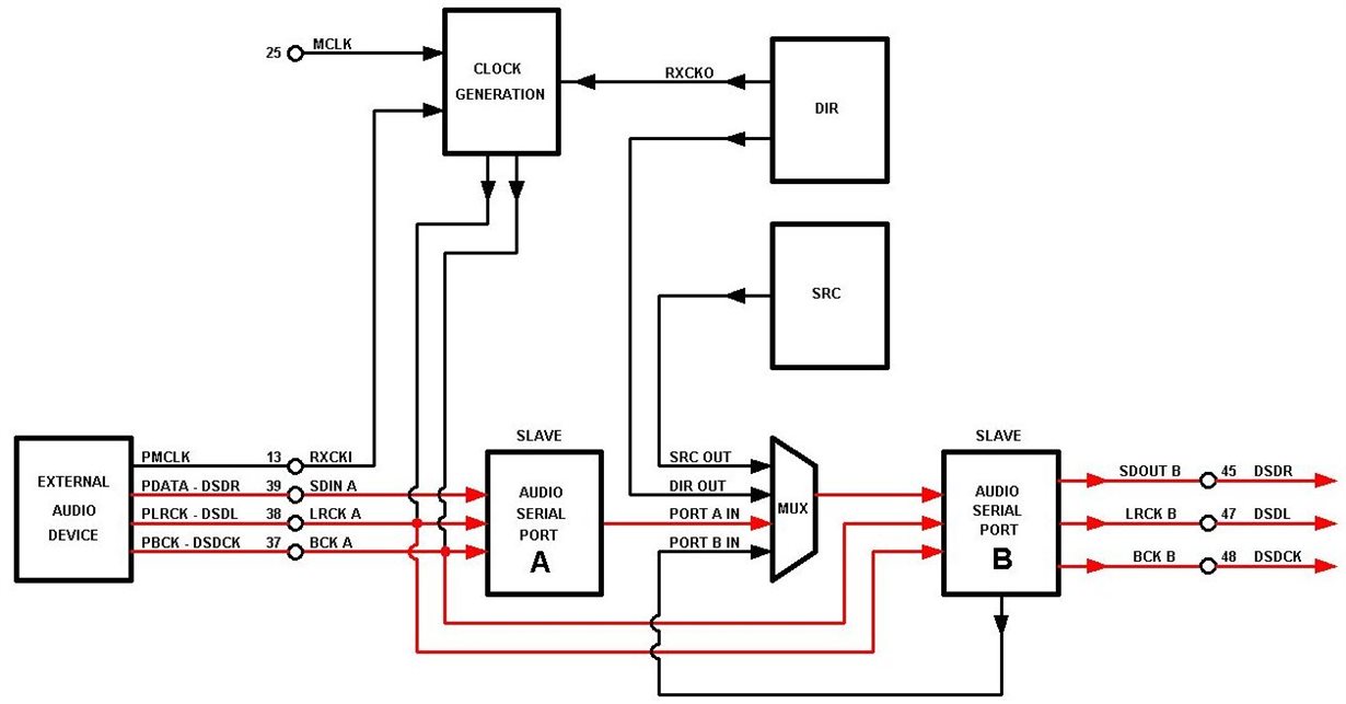
    I was wondering if the same applies and for SRC4392 if PORT A is used as input for DSD over PCM and PORT B used as output. It is of big importance as in my project i use the I2C control mode and the only device with exclusive SPI control is the SRC4193 while the SRC4392 can be managed with I2C. Is not so much a matter of money, as the cost of an SRC4193 plus a I2C to SPI bridge (to make economy in MCU I/O ports) is just 3 Euros lower than the SRC4392. Additionaly the SRC4392 offers better performance. Simply i am not sure that i have understand well the bus routing within the SRC4392, although i came accross the datasheet many times. My problem is a USB2.0 audio interface, compatible with both PCM and DSD over PCM formats, which provides these outputs: a) PCM_DATA_OUT / DSD_R b) PCM_LRCK / DSD_L c) PCM_BCK / DSD_CLK. According to the block diagram (Figure 61. "Audio serial port block diagram" of SRC4392 datasheet) the PCM_DATA_OUT / DSD_R can be passed directly from the PORT A to the PORT B through the Data Source multiplexer of PORT B. The issue is what applies to the LRCK and BCLK clock lines. Here is an extract from the SRC4392 manual, regarding the audio serial ports operation:

    The SRC4392 includes two audio serial ports, Port A and Port B. Both ports are 4-wire synchronous serial interfaces, supporting simultaneous input and output operation. Since each port has only one pair of left/right word and bit clocks, the input and output sampling rates are identical. The left/right word clock (LRCKA or LRCKB) and the bit clock (BCKA or BCKB) may be configured for either Master or Slave mode operation. In Master mode these clocks are outputs, derived from the selected master clock source using internal clock dividers. The master clock source may be 128, 256, 384, or 512 times the audio input/output sampling rate, with the clock divider being selected using control register bits for each port. In Slave mode the left/right word and bit clocks are inputs, being sourced from an external audio device acting as the serial bus master.


    Accordingly PORT A (used as input) must be configured as slave. What applies to PORT B to be used as output? Master or Slave? I am sure that there is some way to pass the BCK and LRCK derived from port A directly to port B. My assumption is that also PORT B should be configured to work in slave mode to not be dependable on the internal PLL clock but then the LRCKB and BCKB will become inputs (???) I am not sure on this. Based on my assumption i designed the attached schematic. With red lines is represented the assuming routing for DSD formated data. For PCM data is desirable the async mode, i.e. the upsampling in high rates and the re-clocking.

    Any help will be much appreciated

    Thanks