This thread has been locked.

If you have a related question, please click the "Ask a related question" button in the top right corner. The newly created question will be automatically linked to this question.

TLV320AIC3104: How to select the switch DACR-R3

Part Number: TLV320AIC3104


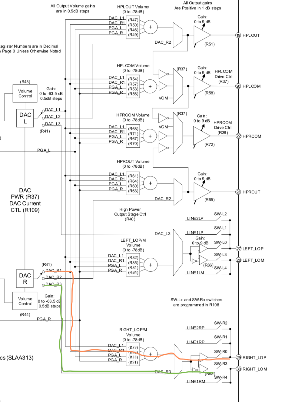
I need some help with the codec (TLV320AIC3104). I´m trying to apply a signal in MIC2R/LINE2R input in order to see it with the osciloscope in RIGHT_LOP/LOM output. The problem is that I dont know very well how to route the signal to see it in the output. I apply some PGA gain and some AGC gain in the right channel after that (seeing in the data sheet) the signal should go to the the Audio Serial Bus Interface to the microprocessor and then comes back to re right channel. The key is in the DACR in which I should choose the route between R1,R2 and R3. In my case, as I want to see the signal in RIGHT_LOP/LOM I should choose DAC-R3, the thing is that the only register I´ve seen to modify is the DAC-R1 (reg.92) and I don´t see any with DAC-R3. How can I do that?

Thanks in advanced.

  • User,

    There are a couple of ways to do this.

    page 0 register 41 has the DAC output path selection. Using the DAC_R3 path is the most direct path, but the DAC_R1 path can also be used.

    For DAC_R3 path:

    w 30 00 00 # select page 0
    w 30 29 10 # left DAC ->DAC_L1, Right DAC-> DAC_R3
    w 30 5D 09 # power up Right_LOP/M output and unmute.

    for DAC _R1 path:
    w 30 00 00 # select page 0
    w 30 29 00 # DAC_R1 and DAC_L1 path are chosen by default.
    w 30 5C 80 # route DAC_R1 to RIGHT_LOP/M output
    w 30 5D 09 # power up Right_LOP/M output and unmute.

    As I mentioned before, the DAC_R3 is themes direct path, but it will also have more out of band noise, so consider using an external LPF especially if you are connecting the Right_LOP/M output to a Class-D amplifier.
    the DAC_R1 path allows for the use of the analog mixers, and there is some built in signal conditioning that decrease some of the noise. the THD and in-band noise will be marginally higher.

    best regards,
    -Steve wilson
  • Hi Steve thanks for your response.  As you mentioned before I prefer to use the DAC_R1 path due to the noise problems. I thought that I couldn´t use this path because if you look at the drawings there isn´t a path in the DACr output that leads you to the Right_LOP/M only the DAC-R3.

    In the DAC path details you gave me in the answer, what does the numbers "w 30 00 00" mean?

    Regards,

  • User, 

    I've shown the two paths in the image below.  The DAC_R1 path in orange, and DAC_R3 path in Green:

    regarding the number format,  This is the format the evaluation module GUI uses to program the device.  

    w - write

    r- read

    d- delay

    the first hex pair is the device address,  the second pair is the register number and the third pair is the value. 

    one slightly confusing aspect is that the device address is shifted one bit to the left.  so for the AIC3104, the address is 0x18.  But shift that one bit and you get 0x30. 

    so w 30 01 80 means write to the device associated with the I2C address 0x18, register 0x01, a value of 0x80. 

    make sense?

    best regards,

    -Steve wilson

  • Hi Steve,

    As I can see your drawings are different than mine. I have the datasheet revised in December 2016. Is there any updated datasheet? You can see a screenshot attached (If I managed to upload it) in which you will see that the path from DAC-R1  goes only to LEFT_LOP/LOM.

  • User,

    This is an error in the block diagram.  I am working on a datasheet update that updates the block diagram, clarifies some of the function descriptions, and makes some minor corrections to the register map etc... I can provide you with the updated block diagram. This new diagram has considerably more detail, I find it to be very useful.  I hope you do too.

    best regards,

    -Steve Wilson

    0160.TLV320AIC3104_Functional_block_Diagram_With_Registers.pdf

  • Thanks. The new block diagram is more useful.

    Regards,

  • User,
    I'm glad you find the diagram useful. If you don't mind, please click the "this solved my issue" button.

    best regards,
    -Steve Wilson