


In our current design PCM2705DB chip is going to be used as the standalone USB to S/PDIF Converter device only.
No analog outputs and external custom descriptors EEPROM will be used.
The device supply is in the BUS-powered mode only.
No SPI bus will be used.
There are some questions when comparing the schematic given in the DEM-PCM2704/2705 EVM, SLEU049A, page 4 and the PCM2705DB datasheet schematic (page 28):
1. Is it absolutely necessary to use following components R12, R13, R16, R17, R18 (the reference designators are from the DEM-PCM2704/2705 EVM, SLEU049A , page 4) in the our design?
The datasheet schematic of the PCM2705DB has no that components used.
2. The PCM2705DB IC pins Vccl, Vccr, Vccp are shorted together by jumpers when the PCM2704/2705 EVM is using in the BUS-powered mode.
These pins are not shorted together in the IC datasheet schematic
It is possible do not short them as it is pictured on the datasheet schematic?
3. Can the HOST pin be connected to Vdd as it is in the IC datasheet schematic?
4. Can we use the PCM2705DB IC in our application based on the PCM2705DB datasheet schematic only (for low parts count)?
Will the device reliability be good then?
As an example it is possible to find some designs in the web such as:
----------------------------------
USB-to-S/PDIF Converter
http://www.hagtech.com/images/hagusbschem.gif
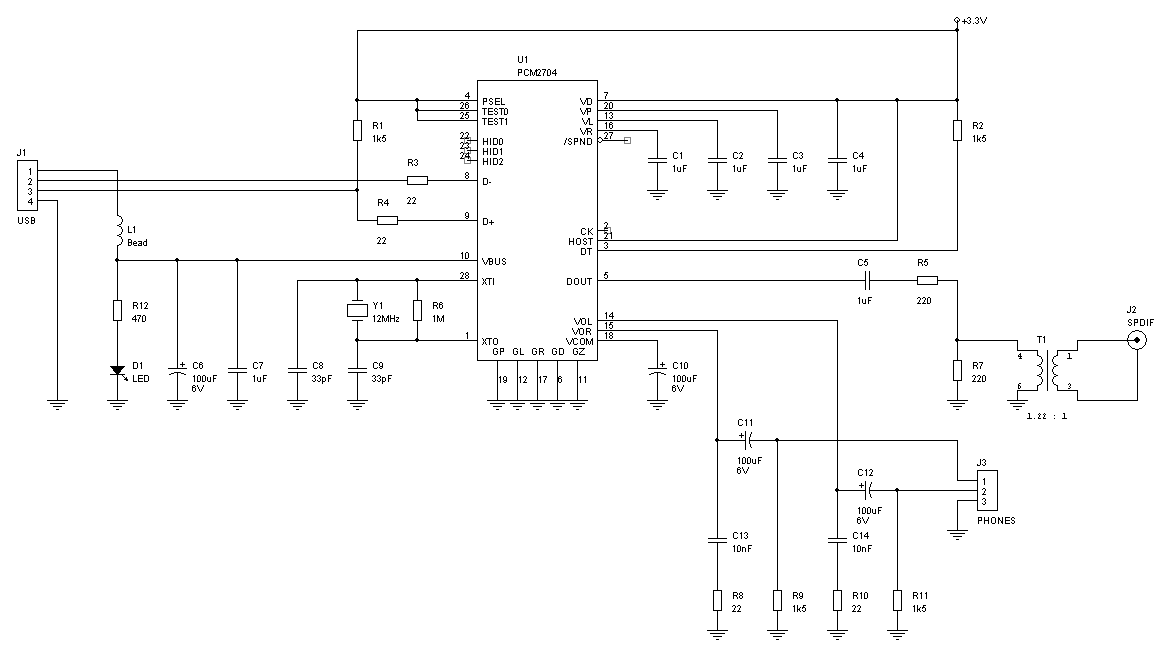
http://www.hagtech.com/hagusb.html
----------------------------------
The chip is PCM2704DB.
Device it is designed on the datasheet schematic only (not on the DEM-PCM2704/2705 EVM schematic).
That device is operable.