This thread has been locked.

If you have a related question, please click the "Ask a related question" button in the top right corner. The newly created question will be automatically linked to this question.

LM48100Q-Q1: Default register values and How to write

Part Number: LM48100Q-Q1


Hello,

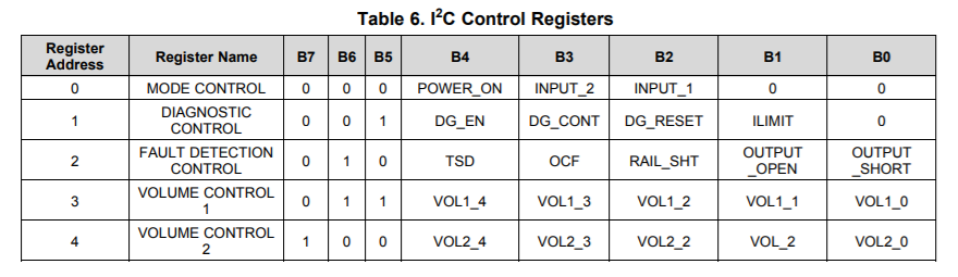
Would you please show all the default values of the registers? it is not clear at the power_up if POWER_ON is 1, the default volume, and if INPUT are on or off.

Would you please advise how to write the registers. In Figure 14 of p.17, there is not register address is involved. Should the user write all the 5 bytes of the register at once? I mean the sequence below:

<DEVICE ADDRESS W> ACK <REGISTER DATA0> ACK <REGISTER DATA1> ACK <REGISTER DATA2> ACK <REGISTER DATA3> ACK <REGISTER DATA4> ACK STOP 

Or can a specific register address be selectively accessed somehow?

Thanks.

Regards,

Oguri (TIJ automotive FAE)

  • Hello, Oguri-san,

    The register address is determined by the register data as shown in the "Example Write Sequence" figure of datasheet.

    First, the device address must be sent. This device is composed by two different addresses that depends of B1. So, the two options are 1111 100 + R/W bit and 1111 101 + R/W bit.

    Then, the register data is sent with the register address (bits B7 - B5) and the register data (bits B4 - B0). Bits B7 - B5 are used to select the register to be written as shown in the table below:

    Regarding the default value, this information is not specified in the datasheet. However, all the bits should be '0' as default state.

    Best regards,
    Luis Fernando Rodríguez S.

  • Hi Luis,

    Thanks! This is quite an unusual scheme.

    Another question is, can the write transaction be done for multiple bytes at once like I wrote in the original post? That is like doing below to write all 5 registers. Or it must be one by one?

    START <DEVICE ADDRESS W> ACK <REGISTER DATA0> ACK <REGISTER DATA1> ACK <REGISTER DATA2> ACK <REGISTER DATA3> ACK <REGISTER DATA4> ACK STOP

    Regards,
    Oguri
  • Hi, Masatoshi,

    I agree, the I2C scheme is a little different from the normal usage.

    Since the register data also contains the registers address, it is not possible to write all 5 registers consecutively. You must write them one by one.

    Best regards,
    Luis Fernando Rodríguez S.