Because of the Thanksgiving holiday in the U.S., TI E2E™ design support forum responses may be delayed from November 25 through December 2. Thank you for your patience.

This thread has been locked.

If you have a related question, please click the "Ask a related question" button in the top right corner. The newly created question will be automatically linked to this question.

SRC4190-Q1: The relationship between RCKI and tRCKIH/tRCKIL

Part Number: SRC4190-Q1
Other Parts Discussed in Thread: SRC4190

Hi, Team,

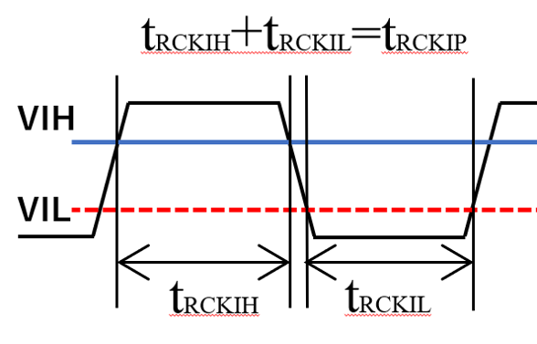
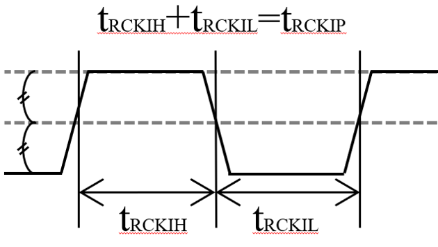
A bit confused about tRCKIH, tRCKIL in Figure 2 of the datasheet because it does not show DC level as well.

Therefore, there are two ways to interpret this:

1. From the datasheet, Hi and Lo level voltage is defined as 0.7*VIO, 0.3*VIO, respectively.
Therefore, to be exact, tRCKIH, tRCKIL should be depicted as:

2. Just like depicted in Fig. 2, the border is drawn in the middle of the amplitude.

Could you please tell us the correct understanding?

Thanks and Best Regards,
Masaru Oinaga

  • Hi Oinaga-san,

    The purpose of Figure 2 in the SRC4190 datasheet is to visually describe the maximum clock speed and the duty cycle limits of the clock which is 50MHz and 60/40 duty cycle.  Ideally you would have 50/50 duty cycle.  Does that help to clarify things for you?

  • Hello, Tom,

    I understand about the duty cycle which would be 50/50 ideally.

    My question here is that if you look at the diagram, when the waveform is in tRCKIH, it seems to be above the center of the RCKI.
    Since it does not provide any information about the y-axis, I wanted to make sure about the DC level of each tRCKIH/tRCKIL.

    Since the reference clock signal can be a source of noise, the customer would like to shape the waveform closer to sine waves instead of rectangular waves using a damper resistor.
    If tRCKIH and tRCKIL is determined as above and below the center line of the RCKI, respectively, they would like to make the amplitude as small as possible.
    (That is also why I mentioned about Hi and Lo level voltage is defined as 0.7*VIO, 0.3*VIO, respectively, in the original question.)

    Thanks and Best Regards,
    Masaru Oinaga

  • Hi Oinaga-san,

    The pictures in the datasheet are there as a visual aide to help you understand what the physical timing parameters apply to.  You should focus more on the actual timing specifications rather than the drawings.  The 70% and 30% levels are the valid logic high and logic low levels, so if the picture would have been drawn as a perfect square wave, would that make things clearer for you?

    Dampening the reference clock with series R and/or R/C would help with noise (EMI, over/undershoots, coupling), but I do not have any data to show the impact of making this input a sinusoidal wave.