Hello,
Our customer plans to use PCM1840 in slave mode.
To review their inputted BCK clock timing from DSP, which specification should we referred?
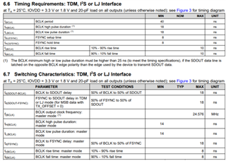
Section 6.6 Timing Requirements noted “all outputs”, we expect this specification is in Master mode PCM1840 will output PCM data as following timing specification. Is that correct?
6.6 Timing Requirements: TDM, I2S or LJ Interface
at TA = 25°C, IOVDD = 3.3 V or 1.8 V and 20-pF load on all outputs (unless otherwise noted); see Figure 3 for timing diagram
One more curiosity is definition of rise and fall time on the datasheet, for output node 10-90% is reasonable.
However for input node as Slave mode BCK pin input, clock timing might be defined by Vth H(max) and Vth L(min), it is not 10%-90%. Can we read the specification with this definition in Slave mode?
tr(BCLK) BCLK rise time 10% - 90% rise time 10 ns
tf(BCLK) BCLK fall time 90% - 10% fall time 10 ns
Because, mass production products have dumping resistors for those clock lines. Rise and fall time became longer to get better EMI characteristics.
Regards,
Mochizuki