This thread has been locked.

If you have a related question, please click the "Ask a related question" button in the top right corner. The newly created question will be automatically linked to this question.

PCM1773: POR start up seq

Part Number: PCM1773

PCM1773起動時波形.pdfPCM1773_Audioクロック_HighStart.pdf

Please check two files.

file1:

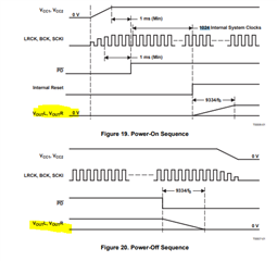
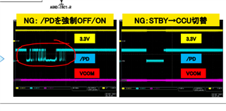
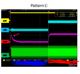
PCM1773起動波形.pdf --> Show customer is getting start up failure on several units.  Waveform shows both good and bad case.
I already confirmed VCC1/2: 10uF + 0.1uf , VCOM 10uF near IC location following datasheet
Customer tried PD hardware RESET but it seems not working.  I suppose somthing thermal shudown or another protection was working that why not PD reset did not work.  please check the cause of issue and suggest any POR sequence?

File2

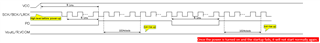
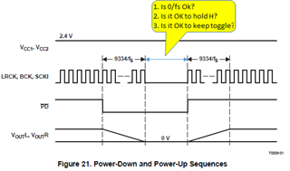
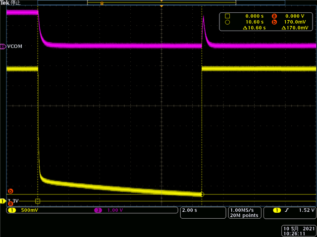
PCM1773_Audioクロック_highstart.pdf
My customer took startup seq waveform as attached.  Customer is concerning about Audio clock high start may have been influenced to device function as negative impact.  Please check attached waveform and let me know your comment? More detail information or If you have any questions, please let me know.

  • Hi Yoshimuri-san,

    I will review this today.

    Thanks,

    Paul

  • Dear Paul-san

    I am a its customer.

    Please let me know these answer ASAP.

    Best Regards.

    Hiroki Kurosaki

  • Hi Kurosaki-san,

    Is the I2S input valid when the /PD is set HIGH in these cases? The device requires SCK to re-initialize after PD has been set low.  Could you annotate the images in PCM1773起動時波形.pdf so that they show when the SCK input is valid and active?

  • Hi Paul-san,


    I'm Kurosaki's colleague. We have two issues to ask.

    The first one occurs when Power is turned ON, this WFM is shown in the left side of PCM1773起動時波形.pdf. In case of NG (left bottom picture of PCM1773起動時波形.pdf), we cannot get the audio data from your device. The difference from OK case is VCOM. And both OK and NG case, we did same Power ON sequence which is shown in PCM1773_Audioクロック_HighStart.pdf. In this figure, you can see the relation between VCC, /PD, VCOM and SCK.


    At first, we want to know why we sometimes cannot get the Audio from your device, means VCOM is still low after /PD goes to High.


    The second one occurs when Power OFF/ON, this WFN is shown in the right side of PCM1773起動時波形.pdf. I think you ask SCK input timing in this case, but do you have any idea about the first issue ?

  • Hi Yamato-san,

    My suspicion is that that the LRCK, BCK, and SCK are not fully valid when PD goes high.  We have a requirement of 1ms of valid LRCK/BCK + SCK data.  The PCM1773_Audioクロック_HighStart.pdf file shows that SCK is high, but it does have over 1ms of data before PD goes high, so that is not a problem.

    For the other file, we cannot really see.  I think they should first monitor all 3 I2S clock lines at startup to see if they are synchronized and valid before the PD signal rises.  If the clock is irregular or missing, I think it could cause this.

    Thanks,

    Paul

  • Hi Paul-san
    I'm Kurosaki's colleague too.
    I have some questions.
    1)Is PD effective only when the power is turned on?
    2)Does PD work again and again after all inputs are stable, even if it is in an abnormal state when the power is turned on?
    3)Is VCOM controlled only by PD?
    4)When VCOM is controlled by other than PD, the timing when the VCOM voltage starts to rise is how many clocks after PD changes to High.
    5)Why does the VCOM voltage rise even though the PD is low when the power is turned on?
    6)Why does the PD low period need more than 1ms after power and clock are valid?
    7)Is there a way to check the operation of INTERNAL RESET?
    8)I think the 1024 clock period initialization sequence has been running since PD changed to High, but is there a possibility that the sequence will get stuck?

  • Hi Fujiwara-san,

    1. I am not sure what you mean by this question.  If you were to assert /PD low at startup, the device would stay in its reset state until /PD was powered on.

    2. My understanding is that two conditions must be met for the device to exit the reset state:

            1. The /PD signal must be high

            2. There must be a valid I2S input applied to the device for a period of 1024 SCK periods.

    3. The VCOM is controlled by the reset state of the device.  You can use these same images to represent VCOM (same behavior as VOUTL/VOUTR).

    4. Please my response to no. 3.

    5. I am not sure why this customer is seeing that behavior.  It could be expected, but I do not have an evaluation tool to confirm.  It could be possible that the device requires the presents of SCK for it's POR circuit to operate.  This could be why the SCK signal is shown on the "power-on sequence" figure. 

    6. It probably needs a millisecond to initialize its digital state machine and start the delta sigma modulator.

    7. I do not know a way to verify the device state.  This device does not have a digital interface.

    8. I am not aware of any known issues with this device.  It could be possible if there is some kind of brown-out state or inconsistent clocking, but I am not aware of any particular behavior.

    I have answered these to the best of my knowledge, but I recognize that the customer's images show a different behavior than what I am describing, so I think it is necessary to look closer at the exact conditions during the failing systems startup.

    Can they collect or confirm that all of the I2S inputs are valid (SCK, BCK, LRCK) before PD is set high?  

    Can they clarify what PD behavior is happening here:

    I also see significant digital cross-talk on the PD and VCC line.  This could just be from the oscilloscope, but I would be worthwhile to see if there could be significant noise on the PD signal that might be causing intermittent behavior.

    Thanks,

    Paul

  • Hi Paul-san

    Can they collect or confirm that all of the I2S inputs are valid (SCK, BCK, LRCK) before PD is set high? >Yes,it is all inputing.

    Crosstalk is a measurement environment issue.It has nothing to do with this issue.

    The meaning of Q1 and Q2 is below.

    (I asked a question because if the power is turned on and the startup fails, it will not operate normally no matter how many times the PD is lowered.)

    Thanks,

    Fujiwara

  • Hi Fujiwara-san,

    Is this failure repeatable on every device? And does a failing device recover is the HIGH SCK/LRCK/BCK condition is removed at startup?

    I am trying to determine if this is some kind of specific device behavior, or a behavior that can be found on every device.

    I am very limited in the amount of information available for this device due to its age, so I am not sure if can confirm if this behavior is expected.  If the behavior can be found on every device and the startup sequence can be modified to prevent this condition, then that would likely be the solution.

    Thanks,

    Paul

  • Hi Paul-san

    I'm using multiple devices, but the probability of occurrence is high only for a specific channel.

    At startup, I tried the Low SCK / LRCK / BCK condition, but it didn't solve the problem.

    Even if the first power-on reset does not work, it is recognized that if PD is performed after stabilization, it will operate normally.

    However, I am having trouble with PD not working this time.

    Please continue to support us as to what measures should be taken to solve the problem.

    Thanks,

    Fujiwara

  • Hi Paul-san

    There is confirmation in the power-down and power-up sequences.

    Thanks,

    Fujiwara

  • Hi Fujiwara-san,

    1. 0/fs delay should be okay.

    2. Holding the clock lines high should also be fine.

    3. Continuously toggling the clocks is okay.

    Does stopping the clocks during the error state, then toggling PD high→low→high, then resuming the clocks get the part out of the error state?

    Thanks,

    Paul

  • Hi Paul-san

    When VCC apply, VCOM is rise together.
    VCOM rising have 3 pattern below.
    Do you know why happen these motion?
    1. VCOM rise a moment.
    2. VCOM rise about 1 second.
    3. VCOM rise continue.

    Your below suggestion is going to checking in a few days.

    "Does stopping the clocks during the error state, then toggling PD high→low→high,
    then resuming the clocks get the part out of the error state?"

    Thanks,

    Kurosaki
    PCM1773_VCOM_RisePattern.pdf

  • Hi Kurosaki-san,

    I am not sure why the VCOM is behaving this way. 

    Do you know why the SCK looks different when the /PD line goes high? Is it changing frequency? Is there addition clocks starting at that same time time?

    Thanks,

    Paul

  • Hi-Paul-san

    It was found that this phenomenon occurs 100% when Power is turned on with a voltage of about 170 mV remaining in VCC1 and VCC2.

    There is no description in the spec sheet.

    Sends VCOM and VCC waveforms.

    Do you think what is happening inside the PCM1773?

    Thanks.

    Kurosaki

  • It is possible that the device is being kept in a brown-out state because the device is not fully powered off.  This would be some kind of unknown startup/POR case.  Is it possible to avoid this condition in your application?

  • Hi Paul-san.

    We must understand correctly brown-out mechanism to avoid this condition in our application.
    In a brown-out state, why is internal reset not active?
    Therefore, I have more two question.

    1) What kind of protection circuit does the PCM1773 have?
    2) Do you have an equivalent circuit of that protection circuit or power(VCC) block circuit?

    Thanks.
    Kurosaki

  • I will respond to this tomorrow.

  • Hi Paul-san

    A prompt reply will be greatly appreciated.

    Thanks.

    Kurosaki

  • Hi Kurosaki-san,

    This device would only feature ESD diodes from VCC to GND that would start to conduct at about 300mV above VCC. Similar diodes would be present on all the pins.  We have limited design input on this device, so I cannot provide specifics.

    I expect that what is happening is that the digital block of the device is not fully resetting due to the slow supply ramp down (or limited supply value), and that is very hard to confirm.  Could some kind additional current path be added to help discharge this line? For example, could a 1k-5kΩ from VCC to GND be added?

    Thanks,

    Paul

  • Hi Paul-san

    Thank you for your information.
    Would you please examine in your laboratory that the digital block is not fully resetting?
    It doesn't matter if it takes time.
    I want a technical answer with measured data about cause of internal reset doesn't working.
    Products with this device have already shipped, but I'm worried about this problem happen in the market.

    Thanks.

    Kurosaki