Other Parts Discussed in Thread: TLV320ADC3100
Hello,
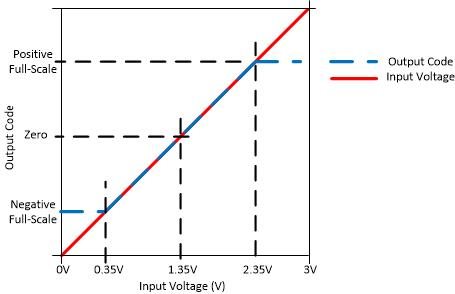
What is the transfer function relationship between the input voltage applied to the TLV320ADC3101 and TLV320ADC3100 devices and the resulting output codes?
This thread has been locked.
If you have a related question, please click the "Ask a related question" button in the top right corner. The newly created question will be automatically linked to this question.
Hello,
What is the transfer function relationship between the input voltage applied to the TLV320ADC3101 and TLV320ADC3100 devices and the resulting output codes?
Hello,
Here is a visual to help represent the ideal transfer function of the TLV320ADC3101. The full-scale input level is 0.707Vrms or 2Vpp ideally, but there will be non-zero gain errors that will shift the curve from part-to-part. The TLV320ADC3101 is specified with a single-ended gain error of 0.7dB typical and there will be a roughly +/-0.5dB distribution around that center value.
The output codes in I2S are standard binary two's complement formatted.
