This thread has been locked.

If you have a related question, please click the "Ask a related question" button in the top right corner. The newly created question will be automatically linked to this question.

LM3886 - Stability when operating as a current source

Other Parts Discussed in Thread: LM3886, TEST2

I hope one of you amplifier gurus can help me with this problem. (I have minimal expirience with current amplifiers)

I have been asked to improve an existing 60Hz current source based on the LM3886. The present design can develop 0-2 Arms, and the goal is to increase the output to 4 Arms. Unfortunately the schematics, layout  etc. for the original source are no longer available.

To get started I reverse engineered the existing circuit and created a new board that I believe is electrically similar to the original design. I say similar because I changed the through hole components to SMT so the layout is now different. The new circuit works under some conditions but will not operate with the desired load. The intended load is non-linear.  I have done some testing as follows:

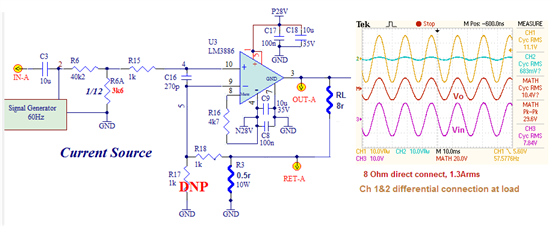
Test 1) output directly connected to an 8 Ohm resistive load:

  • Appears to work well, output waveform is clean and will deliver >2Arms  (SO FAR SO GOOD)

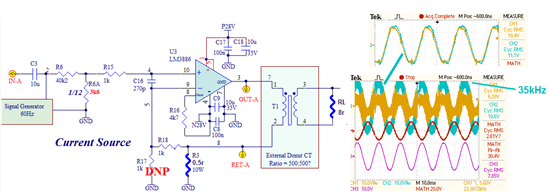
Test 2) similar to test 1, with a 500:500 CT between the amplifier and load:

  • Works to some extent, output contains ~30kHz oscillation superimposed on 60Hz (see below) NEED TO FIX THE OSCILLATION!
  • Oscillation appears to be common mode, (does not appear in CH1-CH2 display)
  • Output level is lower (may need to increase drive when oscillation is fixed.

Test 3) with intended load:

This current source will be used to test a current measurement circuit used in an existing product.  The device to be tested is normally connected to the power system via a 1000:1 CT.  For the production test we use the above current source and a 500:500 CT to drive the DUT. The DUT both measures the current and is powered from the current being measured.

  • Circuit as shown below (same current source but with DUT load)
  • Works to some extent,  output sinusoidal at very low levels (14Vp-p into DUT, very little current)
  • Note: May not be relevant but the power supply rails on the old current source are +/- 40V, while my test setup only  has +/-30V rails (for now, bigger lab supply on order) I don’t think this matters at this point

Increasing the drive quickly causes output waveform to change from sinusoidal to a “squarish” wave. If the drive is further increased, the waveform becomes a square wave and the measurement circuit on the DUT begins to detect the signal at very low levels . If the drive is further increased the amplitude of the square wave increases and then eventually starts to have drop-outs. The new current source can only produce very low levels compared to the original source (~ 0.1A vs. >2A). The lower power supply rails on my new test circuit may be contributing to the problem, but I expect there is more to the problem.  The DUT load is peculiar in that it “harvests” power from the input current circuit, I’m somewhat surprised the old current source is able to drive this load but it does cleanly up to 2A rms.

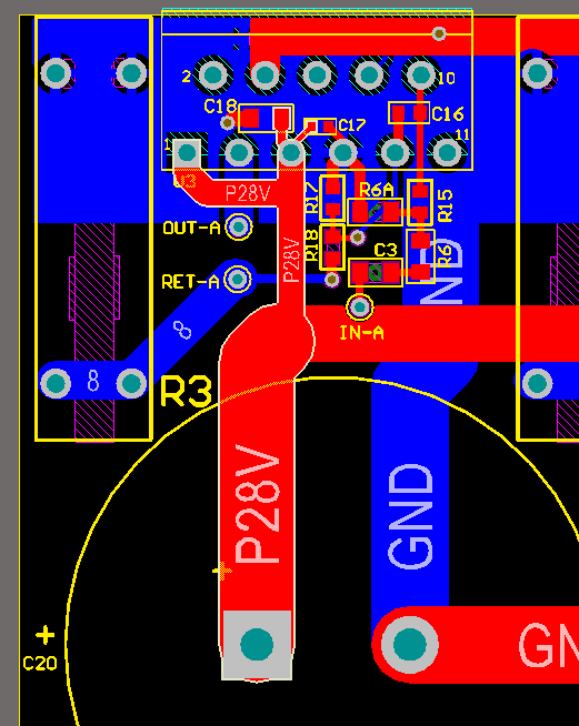
The layout of the new current source looks like this:

I hope one of you gurus can make some suggestions as to how best to approach the problem.

Getting the source stable with the CT seems like the first step.

It's possible that when the power supply rails are higher +/-40 vs. +/-30 the source may be better equipped to drive the strange DUT load as the string of series diodes requires between 10 and 18V to forward bias (depending on current)

Jeff

  • Hi Jeff-san,

    I'll make some comments on your issue.

    For test1 schematic which is loading resistive load, Since the load is resistive, total freq response on LM3886 has no impact.

    We are recommending to set the gain more than 26dB for stable operation.Test1 ckt has about voltage gain of x33 or 30dB from (+) input to amp output.

    But Test2 ckt is different. Primary side of CT is included LM3886 open loop freq response which means CT gives additional phase shift.

    As the result, the device is in unstable mode. To avoide the osc, I'll recommend to add R+C to primary side of CT.

    The value will be, R=50 to 150 ohms and C=0.047uF to 0.22uF depending on your CT inductance. Please check stopping the osc by adding

    those R&C in parallel to CT on test2 ckt.

    For test3 ckt, Please apply same idea as test2 solution.

    I hope to solve your issue.

    Best regards

    T NAOKAWA

  • Toyojiro,

    Thank you for responding to my post.

    Your suggestion works!

    I was able to drive the DUT with just under 4Arms after adding the RC circuit (100 Ohms, 100nF)

    I do have three follow up questions, that I hope you have time to answer:

    1)  How did you calculate the gain of 33?

         (note: Although the original design had a location for R17 on the PCB, R17 is not populated)

    2) If I measure the primary inductance of the CT, should the secondary be: open, shorted, or with the DUT load connected?

    3) At maximum output the resistor in the RC circuit dissipates 15^2/100 = 2.25W. I did a few tests with higher values of R (and found that the the output remains stable with just the 100nF capacitor and no resistor as long as the voltage rails are +/-30Vdc), with less than +/-30V, the output begins to ring as the current is increased beyond about 2A rms. There is an obvious advantage to using the resistor because I can reduce the power supply rails (and hence heat) while maintaining stability. Tomorrow I will find by experiment the highest value of R that will maintain stability while allowing me to decrease the power supply rails. That being said I would like to understand how you determined the R & C values?


    Regards,

    Jeff

  • Hello Jeff-san,

    It was good to hear that it worked well.

    I'll make some comment on your question.

    1) How to calculate the gain of 33.

       Actually the gain of 34 based on following calculation. The gain from (+) input pin to node R3 is 1+R18/R17

    where R18=R17=1K, the gain is "2". And the from node R3 to Out-A is 1+Rl/R3, where Rl=8, R3=0.5, the gain is

    "17". The total gain is "2" x "17"=34.

    2) Connection of secondary side when you measure inductance on CT primary side.

    You will connect with DUT load connect to be influenced the DUT load to primary side.

    3)How I determined the R & C value

    Since you DUT load is very complex model with including non-linear elements, I just used your test2 ckt and

    guessed impedance of CT. The impedance of CT will be inductive load and also you had osc with around 30Khz.

    LM3886 has 115dB of open loop gain and rolling of to around 8Mhz. this time test2 ckt has inductance element in

    feedback loop and adding additional phase shift. With test2 ckt thephase shift may exceed 180deg around 30Khz.

    To recover the phase bshift around 30khz, just adding resister around 100 ohms is OK to stop osc. but current flow this resister will appear on the voltage across the R3. The purpose of R3 is detecting current flow of CT. So the current flow R3 will add error. To minimize the error on the current on R3, I used cap with relatively high impedance at 60Hz and low impedance at above say 3khz or so to recover phase shift around 30Khz.

    So I suggested to take R &C with proper value from the range for actual DUT load.

    I hope to help this explanation for your understanding.

    Best regards

    T NAOKAWA 

  • Toyojiro,

    Thank you for your help.

    Regards,

    Jeff