This thread has been locked.

If you have a related question, please click the "Ask a related question" button in the top right corner. The newly created question will be automatically linked to this question.

OPA1604: TIDU034 questions and possible upgrade solution

Part Number: OPA1604
Other Parts Discussed in Thread: OPA1622, TINA-TI, LME49600, , OPA1644, OPA1612, OPA1602

Hello dear Ti comunnity.

I've got some question regarding TIDU034 design from Ti main site.

More or less they (my questions) are related to common mode distortion and making that circuit less vulnerable? 
If common mode distortion came due to impedance missmatch on IN- and IN+ then we need to make it equal on U1A stage?
We know values of input stage and let's assume that DAC output resistor will be 50-100R.

According to AD743 PDF we need to this :


Is that correct or it does not matter at all in terms of distortion in audio band?

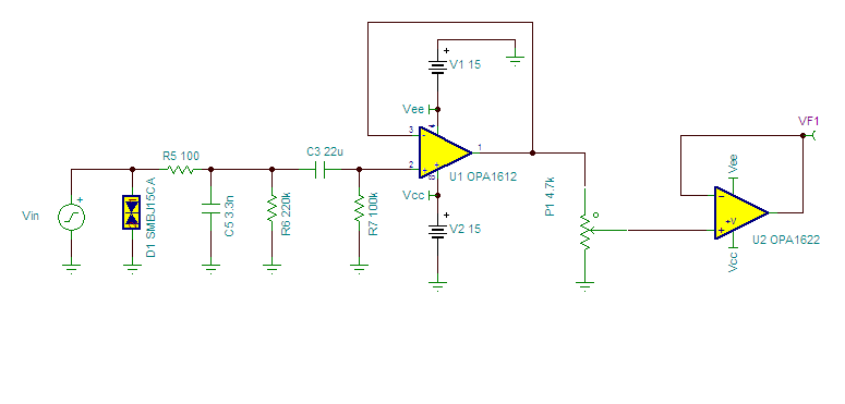
Another question is, could we make R10 22K resistor lower? OPA160x or 164x both are very low input bias current, so I assume I can put lower resistor and it will improve noise as well, or even remove it?
How about putting same value resistor in feedback path of U1C? Circuit is using typical unity gain buffer, but it would not be diffcult to add one resistor between IN- and OUT.

Another question is about output impedance of U1D stage? Is it fixed or is it vary due to taper position of potentiometer?
This is very important because if I connect any buffer in non-inverting mode it will suffer more or less from common mode distortion am I right about this?
If output impedance is variable then should I move U1B inverting stage and buffer U1D output? Due to inverting nature of U1B my phase will be the same as input and my output buffer (which is OPA1622 as a unity gain buffer) will not suffer from common mode distortion.


Am I right all about these or maybe I should find other solution to make everything right? 
If I'm right then I can make some performance upgrades with none or small additional parts which cost almost nothing - this would be nice and preffered.

I've got last question it's related to OPA1622, ATM I'm using it as a standalone buffer outside any global feedback loop.
Should I use OPA160x or OPA164x feedback loop to include OPA1622 inside it? 
If yes why? If not why?

I read some documents about composite opamp stage, but it's more related to CFB opamps or opamps that are actually high input bias current/dc offset etc.

Thank you for your time, have a nice day :)

  • Hi Mateusz,

    1. I'm not sure balancing the two inputs will make much of an impact on distortion. Balancing input impedances is typically done to correct for DC offsets introduced by the input bias current of the op amp, particularly in cases where very large resistors must be used either at the op amp input or in the feedback loop. Balancing isn't going to change the fact that for a noninverting amplifier (or buffer), you're changing the common mode voltage.

    Additionally, as long as you have enough bandwidth, and aren't operating at very high gain, distortion will be reduced by the Aol of the op amp itself.

    2. It's possible to reduce R10, but from a noise perspective, R10 is really in parallel with the two segments of P1. I ran a total noise simulation in TINA-TI, with R10 = 22k and R10 = 2.2k, with no significant difference in total noise level.

    3. AC output impedance will vary somewhat with changes to the position of P1. This output impedance is still flat over frequency, however. The only error I'd expect to see generated by that change in output impedance at different potentiometer settings would be a slight difference in gain from an inverting amplifier stage connected to the output of this circuit. I wouldn't expect to see a change in distortion.

    4. I don't think there's any real advantage to including the OPA1622 in the overall feedback loop. Including it as the output stage of the Baxandall volume control will mean that its AC output impedance will change with volume settings, as mentioned above, which will make absolute volume settings dependent on load impedance.
  • Hi Alex.

    So there is nothing to be done in terms of performance? Or overall design?

    How about moving U1B after U1D stage just to be able to put OPA1622 in his feedback loop? Does it make any real diffrence? 
    Most buffers (standalone like LME49600 or typical opamps) are mostly used with global feedback, rather than standalone.

    Could you tell me how much I degrade THD and noise floor when I replace OPA1604 to OPA1644? This chip is somewhat competetive in price but has higher voltage noise (which will affect dynamic range I supose).
    For this circuit it will be better to stick with hi performance JFET chip or should I look for bipolar one with very low voltage noise? Like OPA1604, or 2x dual ICs like OPA1612 or something else?

    Another question is how low can I go with potentiometer value to not overdrive opamp? ATM I'm using 4.7K so worst case resistance is ~ 1.2K.
    I assume that opamp will be able to handle even lower value pot am I right?

    How about placing 2 gang pot? Output of baxandall will be connected to another gang which will work as a typical (passive) pot with it centre (2 pin) connected to ground.
    It will give me zero output noise when pot will be absolutely muted and will improve control law.

    But how about overall noise of that configuration and THD perspective? If I'm going to use that kind of configuration (which is kinda simple to achive with this desing, it's only a matter of pot) should I put some buffer after passive control or maybe I should leave buffer as it is?


    I know that balancing both inputs will cure DC offset, but I read some desing notes and books about common mode distortion I were thinking about possible solution to avoid it.

  • First, I have to offer a couple of corrections to my post above. 

    1. My simulation of the output impedance of the volume control was in error. While there is some change in output impedance, it is very small. Output impedance simulates well below 100mΩ across the audio band. 

    2. Adding a feedback resistor can improve common mode distortion, as long as your source impedance remains constant. However, in this application the most susceptible amplifier is U1C, which sees a varying source impedance depending on the position of P1. You could add a feedback resistor there, but it would really only be effective at a single volume setting. 

    Buffers inside vs outside feedback:

    A standalone buffer such as the LME49600 typically operates as an open-loop device, which can add considerable distortion. Placing such a device inside a larger control loop will reduce distortion as long as the loop has sufficient bandwidth.

    The OPA1622 has low enough distortion as a standalone buffer that I wouldn't expect significant improvement by wrapping it in a larger loop. 

    Substituting other parts: 

    Either a FET or a bipolar op amp could be used here. The resistor values are small enough that the increased current noise of a bipolar shouldn’t contribute much to the overall noise of the circuit. A FET input op amp will have higher voltage noise, in general. Both OPA1604 and OPA1644 have very low common mode distortion, and all 3 options have very low THD+N in general.

    Our models for OPA1602, OPA1622, OPA1644, and OPA1612 all model noise accurately. To optimize this design for noise, you might want to consider running noise simulations in TINA-TI. We do not model distortion, unfortunately.

    Potentiometer values:

    We have curves for THD+N vs frequency for different load resistances in the datasheets for all of these parts. Keep in mind that the amplifier may be able to drive a smaller resistance, but its distortion will increase while doing so.

    Additionally, at lower resistance values, thermal effects in the potentiometer may need to be considered. It’s possible for these thermal effects to introduce distortion within the resistor itself. 

    2-gang pot:

    Placing a 2-gang pot here would work, but would negate the benefit of using a Baxandall configuration, as you would no longer have a linear-in-dB response for the volume control. If you don’t need that linear behavior, this design could be greatly simplified.

  • So I assume that I can go even lower than 4.7K, to something about 2.5K (~ 600R worst case scenario) am I right?

    When I was talking about 2 gang pot I was refering to this picture :

    If output impedance of U1D is very low then there is no need to use additional buffer, but due to low output impedance of U1D it's not a bad idea to move U1B stage right after U1D, overall gain would not be affected.

    How about making input impedance equal of U1A stage? I will do it just in case :)

    My version is not so diffrent, I just changed some values.

    So here is the question.

    If I've got 220R in series with signal, and then two resistors which parallel impedance is equal to 10kohm + I will include output resistor from DAC which is 50-100R (in most cases).

    Then I assume I need to add all those values and it will give me my RB, right?

    How about CS? I've got those TVS diode which is ~ 1.5nF and then a second LPF with 1nF.

    I've got another question which is related to differential amplifier desing.
    I where thinking about using it to feed enable pin of OPA1622, but it's a good idea to work with those with gain less than one?

    I want to feed both inputs with my power supply voltages (symetrical 18V, or I can use some voltage dividers) to achieve output voltage less than 1V.

  • Hi Mateusz,

    Again, you may be able to reduce the potentiometer value, but you'll likely be trading a small amount of thermal noise for some amount of distortion, due to increased loading on the op amps.

    The dual-gang potentiometer circuit is a valid circuit, but does defeat the purpose of using the Baxandall circuit, since your volume control won't be linear-in-dB anymore. If having a linear-in-dB volume control is not important for your application, using a circuit like the following may be a better option.

    OPA1612 and OPA1622 in this schematic could easily be replaced with another op amp if desired.

    Regarding common mode distortion, John Caldwell goes into more detail in the following two articles: 

    http://www.ti.com/lit/an/slyt595/slyt595.pdf 

    https://e2e.ti.com/blogs_/archives/b/precisionhub/archive/2014/07/15/resistors-in-the-feedback-of-a-buffer-ask-why 

    So long as your source impedance is low, it likely wont be an issue. In this case your source impedance would be the sum of your DAC output impedance and your series resistance. 

    The TVS diode should be included if the input of this circuit connects to the outside world (in the application note, an RCA connector provided the input signal from elsewhere). If your DAC and volume control are on the same board, there shouldn't be a problem with leaving this out. 

    Similarly, the input filtering in the application note was provided to block environmental EMIRR, you may need to add a reconstruction filter on the output of your DAC, but this may follow a different design than in the application note. Your DAC will likely provide a recommended application circuit in its datasheet. 

    I am not sure I understand your question on differential amplifiers and the OPA1622. 

  • So if I understand rigth - if I've got 50-100R resistor in series with DAC output opamp and then followed by 220R in amplifier (due to LPF) then my RB (according to 1st picture in my thread) will be in range of 270-320R am I right?

    How about CB then? Let's use values from your last picture.
    I've got some free space, so adding two passive components to balance impedance of U1A stage is not a problem.

  • Hi Mateusz,
    That's correct. For a combined 270Ω - 320Ω in series with the input, you'd want a similar resistance in the feedback path.

    Adding capacitance to the feedback is typically only done when large resistors are added, to perserve stability, and won't result in an improvement to common mode distortion.
  • But it will match hi frequency impedance when I add those capacitance, am I right?
    BTW should I use some resistor in series with U1D stage? Or it's not needed?
    Traces to OPA1622 are pretty short anyway :)

    If I move U1B stage after U1D (as a inverting buffer) will it lower my output impedance in comparision to U1D stage?

  • My apologies, I failed to consider the input filter. In that case, your feedback capacitor should match your capacitor to ground in the input filter.

    If you're adding an OPA1622 as a buffer after U1D, I don't think there's much benefit to adding resistance there. Both inputs of the OPA1622 would be looking into low impedance sources (op amp outputs), with very little mismatch to induce common mode distortion.

    Output impedance of both configurations should be very close.
  • I think it will be my last question ;)

    How about decoupling? Should I place a capacitors between VCC and VEE when my load is connected to GND?
    It's hard to find a good answer, some people are placing it just in case, some placing it when handling balanced signals/loads.

    I'm just curious about it ;)
  • Placing decoupling between Vcc and Vee isn't a bad idea, but may not be necessary if most currents are returned to ground. I think the only tradeoffs are cost of additional capacitors and PCB area.
  • Does it change anything?
    Should I pick 100nF or something lower/higher?
  • It would help if supply currents or supply noise had a differential component, as the normal decoupling caps to ground would be considered in series to such a signal. Adding a capacitor across the supplies would increase the capacitance between them.

    If you're using 100nF capacitors for decoupling elsewhere, I'd reuse those here as well.
  • I've got some question regarding ground and power supply.
    Does it make any diffrence when I'm using TPS7A4701 and TPS7A3301 to add series resistance or inductor to power up opamps?

    How about splitting ground for analog signal and power (right now I'm using common ground) I know that it's often used for mixed signal or when some hi freq DC-DC are used, but maybe it will give a more quiet ground?
  • You could possibly add a series low-pass filter, either RC or LC, after the LDO's output capacitor. This might help with conducted noise from the power supply at higher frequencies, but I suspect that the LDO's PSRR combined with the op amp PSRR will be sufficient, especially within the audio band.

    As long as your supplies are relatively quiet, I don't think it's necessary to split your signal and power grounds in the analog section.
  • But spliiting ground to two polygons and connecting it in one place (lets assume board center) is not that bad idea.
    It will not harm anyway?

    If I'm using few opamps I assume everyone should be decoupled between VCC and VEE? Or one bigger cap near regulators will be sufficient?
  • Hi Mateusz,

    Splitting the ground plane can be a little dangerous if you aren't careful about routing, since it can create large loop areas which can increase noise in your design.  So long as you're careful with your routing, though, it shouldn't be a problem to split your analog and digital sections. Just make sure that you don't have traces crossing that split, and make sure you tie your planes together at some point to minimize loop currents. 

    For more information, I'd recommend Henry Ott's Electromagnetic Compatibility Engineering as a reference for signal integrity questions. 

    For decoupling, best practice is typically to place a 10nF-100nF ceramic capacitor near each active part (unless you have a number of active parts very close together).

  • Hi Mateusz,
    I hope this thread has resolved your questions. I'll go ahead and mark this as closed, but if you have any other questions, you can reply below to reopen it, or submit a new post on E2E and we'd be happy to assist.