This thread has been locked.

If you have a related question, please click the "Ask a related question" button in the top right corner. The newly created question will be automatically linked to this question.

PCM5100A: Poor output sounds.

Part Number: PCM5100A
Other Parts Discussed in Thread: PCM5100

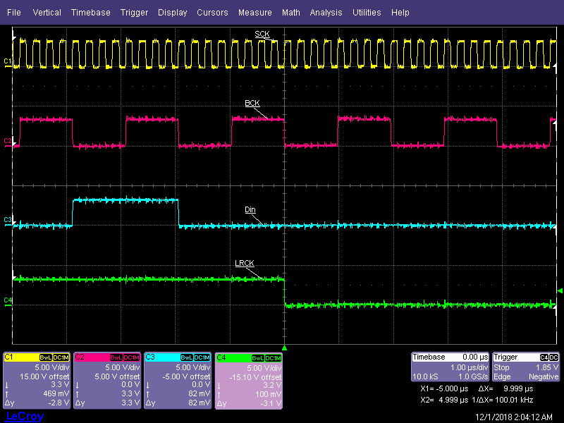
Please review ( hardware sanity check) PCM5100 schmatic.docPCM5100_output.m4athe attached PMC5100A schematic and listen to the m4a sound file.

  • Hi Clayton,

    It is difficult to determine the issue based on the audio file, but you should check a few things. First - verify that the I2S data is valid and in the correct format (I2S). You are using the device in 3-wire mode, so ensure the sample rate is supported (Table 11 in the datasheet). You also have the XSMT pin disconnected. If you are not using the XSMT functionality, the pin should be set high. It could be that the pin is floating and causing an intermittent mute condition. Verify that you see ~-3.3V on VNEG when data is being applied.

    Let me know what you find,

    Thanks!
    Paul
  • Hi Paul, thank you for your work. I am a hardware engineer working off site with two other engineers (hardware & software). If it is possible we would like to setup an conference call with you to resolve this PCB5100A issue.

    Clay
  • Hi Clayton,

    A conference call is possible, but before the call I would still like to see the concerns I mentioned above to be addressed. This would give us a good starting point for the call.
    Feel free to post the results of the investigation here or reach out to me at frost@ti.com

    Thanks,
    Paul
  • Hi Paul,
    Answer to some of your questions from Victor Tikhonov, Lead Electrical Engineer USA Medical Electronix, Inc.


    When we started working on this, XSMT was floating, but Chuck noticed this and for a past few tests it's been pulled up to +3.3V Vdd through a 3.3k resistor (direct tie to Vdd made no difference).

    The VNEG is indeed sitting at -3.3V, which indicated internal charge pump works OK. I believe the VNEG gets generated as soon as Vdd is applied, not just when Din data being applied (fed into Din input).

    The rest of TI's questions about sample rates and such only Chuck can answer.

    If they suggest to verify anything else as far as HW goes, let me know.

    I'll be ready for the call.

    It would be useful to ask TI to email us any "valid" pre-formatted I2S audio sample file to try to play - at least this would rule out one variable.
  • Hi Clayton,

    VNEG should be initialized when there are valid clocks being applied to the device. The charge pump requires a reference clock from SCK (4-wire mode) or BCLK (3-wire mode).

    As far as a pre-formatted I2S sample, not quite sure how that can be provided. Do you have one of the PCM5102EVMs?
    www.ti.com/.../PCM5102EVM-U

    If so, you could bridge the I2S lines to your boards and see if that allows for play back.

    I think the next step on your end would be capture a few complete I2S sample frames. It is difficult to tell from the email if that data is valid. But also note that some I2S sources will apply a 'dither' signal to the output if there is no valid input. For example, SRCs and DIR sometimes do this to ensure that the DACs do not go to sleep mode. This dither signal is usually a few LSB peak to peak centered around bipolar zero. A scope image of the output during this noise event might be helpful as well.

    Thanks,
    Paul
  •  LeCroy3.zipHello Paul,

    Our software engineer, Chuck received the PCM5100 Eval board today.   So hopefully this problem will be resolved soon.

    I have more data from Chuck and Victor below.

    The attached trace file of our problem hardware/I2S bus by color:

    YLW trace is CLK

    RED trace is BCK

    BLU trace is Din

    GRN trace is LRCK

    I see data coming into Din input (pin 14) and it changes as I press the

    K2 button, from periodic blurbs

    to continuing signal, e.g. as if a phrase or a tome being outputted.

    Yet, the OUTL (pin 6) and OUTR

    (pin 7) remain at ground level, as if the PCM5100 is just muted or its output is disabled.

    Here’s a synopsis of the digital data being sent to the PCM5100. All signals come from the PIC32.

    CLK (yellow) is a high frequency clock (4.096 MHz). This is called SCK or MCK in the PCM5100 spec, but Victor is calling it CLK. It’s OK by me.

    BCK (red) or bit clock is used to clock the sample data into the PCM5100, bit by bit. There are 16 bits per sample from a .wav file, originally.

    Din (Data In) is the PCM sample data. It is sent according to the I2S standard. There are two channels of data being sent (left and right channel) and each channel contains the same audio data.

    LRCK (green) is the Left/Right clock. It tells the PCM5100 when the data for a channel starts by it’s leading edge and for which channel the data is sent according to its level. If high, it’s the left channel, if low it’s the right channel.

    The LRCK, BCK and DIN are exactly the same as was sent to the Maxim MAX98357 chip which also supports I2S audio data format. I tested the software before sending it to Victor on our “breakout” board with the MAX98357 and I had good audio at the speaker.

    There are actually 2 versions of the software. One version has audio data sampled at 16KHz, the other has audio data sampled at 32KHz. We used the 16KHz data before with the MAX98357 so you may have heard it. The 32KHz data sounds the same from the MAX98357. The traces in the zip file are mostly from the 16KHz version, but a couple from the 32KHz version, I believe. Note that the frequency of the LRCK is always the same as the sampling frequency and BCK is always 32 x LRCK because we are sending 2 16-bit channels of information. CLK is always 4.096MHz and can server either sampling rate.

    The reason I added the 32KHz version is because it should allow us to eliminate the need for the CLK. At 32KHz the PCM5100 does not require CLK as an input (just like the MAX98357). This is desirable because it frees up a pin on the PIC32, it has lower EMI emission and makes board layout a bit easier. We’ve decided to go with the 32KHz samples and eliminate CLK, if we can get it to work.

    In case you are wondering, the PCM5100 can generate CLK from BCK because it has an internal Phase Lock Loop (PLL).

  • We are discussing this over email now.

    Thanks,
    paul