This thread has been locked.

If you have a related question, please click the "Ask a related question" button in the top right corner. The newly created question will be automatically linked to this question.

TAS5421-Q1: Driving high Z speaker

Part Number: TAS5421-Q1
Other Parts Discussed in Thread: OPA171,

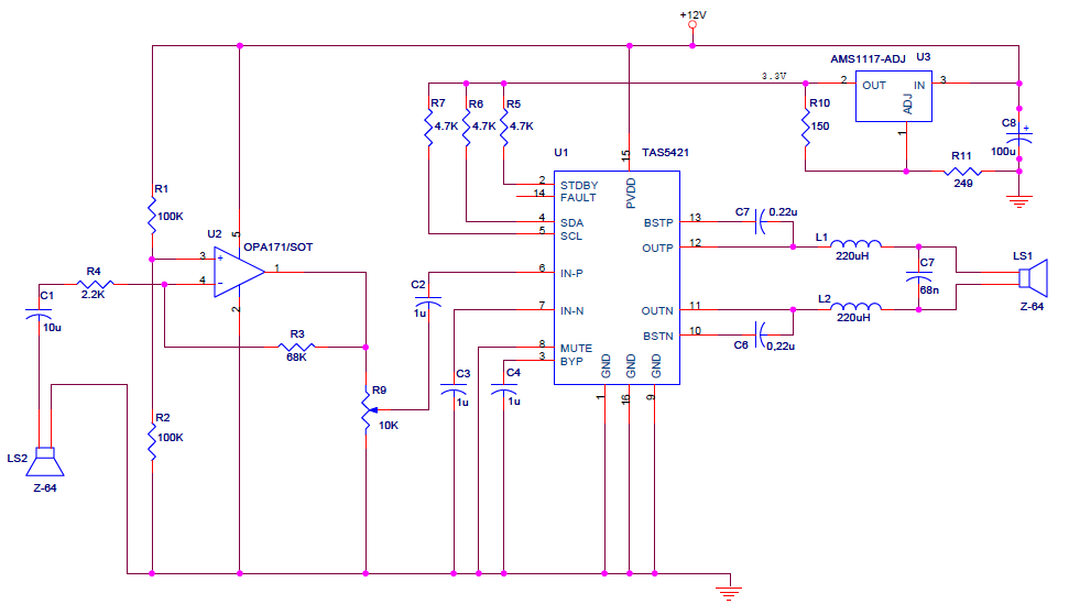
I am trying to drive 64 Ohms impedence speaker using single-ended input. The input source is again 64 Ohms speaker preamplified by ~30dbs using OPA171. The whole system is operating on 12V.

My problem is at lower volume it gives distorted/garbled sound output and then with a slightly larger sound input the volume becomes too high (seems like the chip has AGC internal to it working in reverse fashion).

I tried different output filters and finally selected output filter calculated according to document slou032, with no improvement at all.

Would appreciate the reasoning behind this.

  • Sailesh,

    This is interesting.  I have some questions:

    1. Have you verified that the signal coming from the OPA171 is good? 
    2. Do you have the schematic for the input of the TAS5421?  This is a differential device and needs to be correctly configured for single ended input

  • Thanks for ur fast response.

    1..OPA171 DC output voltage is 1/2 VCC.

    2..Schematic attached...

    Regards,

    Sailesh..

  • Hi Sailesh,
    The potentiometer R9 will have DC current through it and will give you grief. It might not cause this problem, but it should be capacitor coupled at the input the to potentiometer so there is no DC potential across it.
    The LC filter is not the correct type. It need common mode capacitors to ground, as shown in the Datasheet. One across the output does not filter BD modulation properly. This could be giving your speaker problems.
    Fix these two problems, and reply.
  • Dear Gregg,

     I deliberately designed the pot connected to the output of OP amp to reduce unnecessary parts since the extra current drive form OP amp will be 600uA. This OP amp can handle lot more and this shouldn't be a problem.

    I had tried putting common mode capacitors at the output of each L WRT GND but I don't remember the values. I will try inserting capacitors of 10nF at the output of both Ls and let u know.

    Regards,

    Sailesh..

  • The DC through the pot will make the potentiometer create noise when the slider is moved. This is from my experience. And it will get worse with age.
    You will need two 100nF to ground instead of the 68nF. The 10nF will be too low of value.
  • U r right about the scratchiness of the pot. I'll relocate the pot to the output of LS2 and reconnect C2 to the output of OP amp. This will help balance the impedence seen from IN-P and IN-N of the chip to the same value.
    I calculated the common mode caps from doc slou032 which comes to ~10nF but I'll use 100nf too and let u know.

    Regards,
    Sailesh..
  • Sailesh,
    Any update on this thread? I will close this thread and if you respond, it will open it again.
  • Thanks Gregg for ur concern about the issue I am having.

    It's still the same. For ur reference I am attaching the modified schematic:

    I am tied-up in other things but I'll make further analysis using scope and signal generator and get back to u.

    Regards,

    Sailesh..

  • I see that the output inductor is coupled. Can you please send me the datasheet on this inductor? Coupled inductors do not work well on our Class D amplifiers.
  • Due to inactivity, this thread is being closed.
  • Hello Gregg,

    I have limited access to parts in Kuwait hence I fabricated coupled inductor with a ratio of 1:1

    I had got a HTSSOP-16 to DIP-16 PCB designed (in India, on 70u double-sided copper clad board), with thermal pads, to be mounted on bread board.

    The signals were very noisy...most importantly oscillations were generated from OPA171 + the switching noise was also generated from TSA5421 at it's output.

    The OPA171 was made stable by adding 180pF capacitor || with R3. I created two separate  inductors of 90uH for the output of TSA5421 with common mode capacitors of 0.39uF.

    It works very well now with 64 Ohms and 16 Ohms impedance speakers.

    The only part I disliked was, when I set the gain of TSA5421 to 36dB via I2C and re-powered the system, the gain defaulted to 26dB (this is nowhere mentioned in the manual).

    The best part is, the chip has small footprints and very low power consumption.

    Now I can proceed to make a 2 way communication system with electronic switching.

    Thank U for ur help.

  • Sailesh

    The TAS5421-Q1 will lose any changes to the I2C registers when the power is taken away or when the device is placed in Standby mode.  The I2C registers will return to default settings when powered back on.  This is by design.