This thread has been locked.

If you have a related question, please click the "Ask a related question" button in the top right corner. The newly created question will be automatically linked to this question.

TAS2552: TAS2552 I2C slave NAK issue

Part Number: TAS2552

There is a related thread which TI think ist solved, but we are wondering what the solution is?

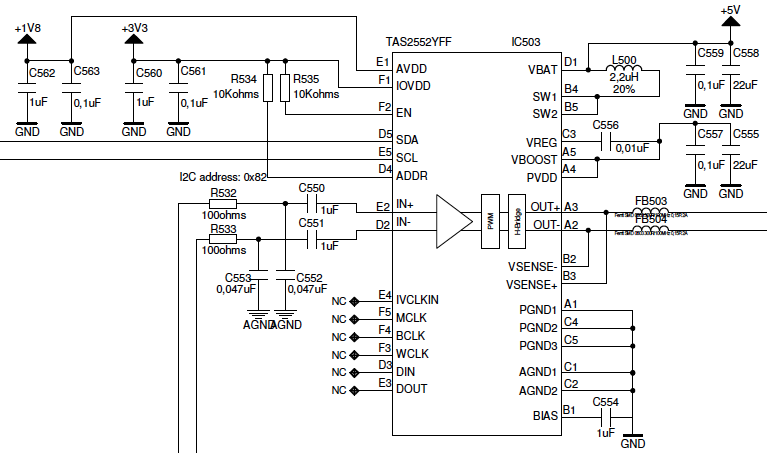
We are having a similar issue where we have boards with the TAS2552 which NAKs I2C requests.

We also had stronger pullups (1.2kohms) which we replaced by the 10k which the EVM uses, however, without any effect.

  • Hi, Michael,

    Do you have this issue when you use multiple TAS2552 at same time? Or even if you use only one TAS2552, do you have a NAKs response?

    I also recommend to take a look at this document for more details about the I2C pull up resistors:

    www.ti.com/.../slva689.pdf

    Best regards,
    Luis Fernando Rodríguez S.
  • Hi Luis,

    thanks for getting back to me and also for the application note.

    We are using a single TAS2552 device. I tried 10kohms as well as our standard 1.2kohms pull-ups, both with the same result: We are getting NAK when accessing the device. I have checked all 3 voltages. We have an analog input and no I2S clock, as per our earlier conversation.

    Best regards,

    Michael

  • Michael,

    Could you provide details about the IOVDD voltage in the device? Have you tried with IOVDD = 1.8V and IOVDD = 3.3V?

    In addition, have you tried with the two supported I2C addresses? When ADDR pin is GND and IOVDD. Do you have the same results?

    Are the TAS2552 and the external processor sharing the same ground plane?

    Best regards,
    Luis Fernando Rodríguez S.
  • Hi Luis,

    the problem is not with the I2C bus but we believe with the TAS2552 not booting: We either get constantly NACK or the chip is working fine, using the same firmware. Especially when the board has been off for an extended period of time we see the NACK issue more often. Once the TAS2552 answers with ACK, it continues to work until the next reset or power cycle. I should mention that the I2S is not used and remains unconnected, as approved by TI before.

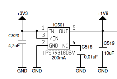
    We use IOVDD=3,3V because the host is based on 3.3V. The 1.8V AVDD is generated using a TPS79318. I have attached our schematic.

    Best regards,

    Michael

  • We tried both I2C addresses, but it did not make any difference. Should we try to GND the ADDR pin?
    And yes, the TAS2552 and the host processor share the same ground plane.
  • Hi Luis,

    the issue with the TAS2552 not always starting is a pressing issue for us, as we have 350 boards ready to ship.

    I have measured the ramping up of the voltages - see below. The cursor marks the Vbat reaching 2.45V.

    Any ideas are appreciated.

    Best regards,

    Michael

  • Michael,

    Is there a way to modify the power supply sequencing in your application? The TAS2552 has a recommended power sequencing since it is sensitive to the voltage changes. Any variation on the voltage may result in a reset state. Probably this issue is associated to a wrong power sequencing and it is causing noticeable issues.

    Could you follow this power sequencing and make sure that each power supply is stable before enable the following power supply?

    1.- VBAT
    2.- IOVDD
    3.- AVDD

    Please let me know if you have additional observations on this.

    Best regards,
    Luis Fernando Rodríguez S.
  • Luis,

    unfortunately, the datsheet does not give precise timings for the voltage sequencing. Do you have more information on this?

    Are all 3 voltages equally critical?

    May ramping of IOVDD  or AVDD start before VBAT has settled?

    For example, how would you drive the EN input on the LDO for AVDD? I have the EN connected to the 3.3V IOVDD, as you can tell from ym schematics..

    Best regards,

    Michael

  • Hi Luis,

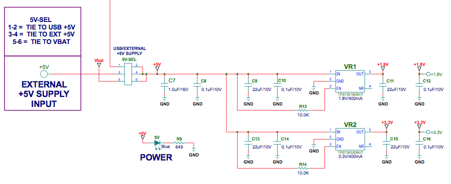
    I checked the EVM again, which I used to develop our schematic: There is no power sequencing on the EVM!

    Please advise.

    Best regards,

    Michael

  • Hi, Michael,

    Usually, the audio devices are tolerant to power supply sequencing. However, there are some cases where the PCB design or the power supplies may affect the device performance or behavior. So, the power sequencing ensures a robust operation.

    It is not specified in the datasheet, but we recommend to have the power supplies stable in the order that I placed in my past post. Ensure that the supply is around the expected value +/- 10% before enable the next power supply.

    If the problem persists even after modifying the power supplies sequencing, please increase the power supplies capacitance to ensure that there's no issue with the power lines (for example, replace the 0.1uF with a 0.47uF and compare the results).

    Best regards,
    Luis Fernando Rodríguez S.
  • Hi, Michael,

    Do you have an update on this? Could you try my suggestions above?

    Best regards,
    Luis Fernando Rodríguez S.
  • Hi Luis,

    we have modified the power supply in order to sequence the rails - see below. However this did not solve our problem.

    Too bad the chip is not defaulting to analog operation when powered up without any I2C configuration.

    We will now X-ray the board in order to rule out any soldering issues.

    Are there any recommendations other than the stencil size as depiced in the data sheet?

    Best regards,

    Michael

  • Michael,

    One more suggestion regarding the power sequencing.

    I see that the EN pin is connected to the IOVDD power supply so both pins power up at the same time. Could you try to powering up the EN pin after the power supplies are completely stable? Wait at least 1ms to power up the EN pin.

    Best regards,
    Luis Fernando Rodríguez S.
  • Hi Luis,

    are you actually in contact with the development enginieers?

    The power sequencing is not specified in the datasheet and not realized in the EVM.

    The same is true for the EN pin, which is also not delayed.

    If any of these measures are mandatory, they should be specified in the datasheet, don't you agree.

    BR

    Michael

  • Hi, Michael,

    I made some calls to the development engineers and these are their suggestions for this case:

    - The power sequencing is suggested in order to avoid some rare circumstances where the device may enter in undefined modes. Even if the device counts with a robust power scheme, having this sequence (VBAT -> IOVDD -> AVDD) will ensure that the registers will be written correctly. In addition, in some rare cases, the device performance may be reduced if the power supplies are not fully stable.

    - Before using or configuring the device, we also recommend to wait for at least 1ms after all the supplies are stable. Then, enable the device through the EN pin and wait for another 1ms. This is a good practice that ensures a good performance at production level.

    - In case of the I2C lines error, we would suggest to verify the capacitance level and try to reduce it as much as possible. The I2C lines are sensitive to high capacitance levels and it may be associated with the I2C communication error in this case. In addition, if you could provide some captures of the I2C lines, it would be helpful to determine the root cause. They can be compared with those of the EVM if necessary.

    - Finally, I would recommend to isolate the device from the rest of components in the I2C lines. I mean, if there are more devices sharing the same I2C lines, it would be helpful to test the communication only with the TAS2552.

    Please let me know if you have questions or comments on this feedback.

    Best regards,
    Luis Fernando Rodríguez S.
  • Hi, Michael,

    Do you have any feedback on this? Feel free to ask any other question about this if you need additional assistance.

    Thank you.

    Best regards,
    Luis Fernando Rodríguez S.
  • Hi Luis,

    thanks for your help. We might have a soldering probllem.

    We will probably do a redesign with a different chip with an easier housing.

    Best regards,

    Michael