This thread has been locked.

If you have a related question, please click the "Ask a related question" button in the top right corner. The newly created question will be automatically linked to this question.

PCM5242: Software mode clock configuration

Part Number: PCM5242
Other Parts Discussed in Thread: PCM5122

Hello,

I've made another hardware spin that allows for software mode configuration of the PCM5242 and am looking to configure the chip to work with an input I2S stream based on 48kHz audio. The datasheet references a SLAC622, which doesn't seem to exist anymore (or maybe never did, if my search of the forums is correct).

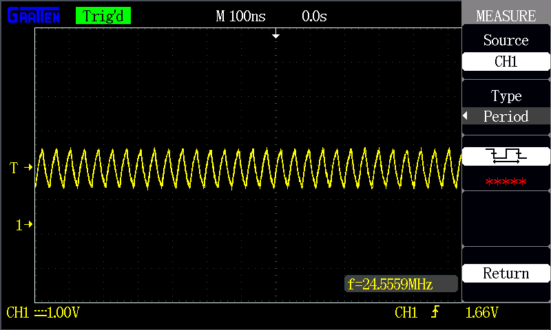
I've been following section 8.8.7 of the datasheet ("Clock Master from a Non-Audio Rate Master Clock"), and have configured the GPIO6 as the input to the PLL w/a 12MHz clock. The PLL is configured to be running at 98.304MHz (R = 1, J = 8, D = 1920, P = 1). I've configured GPIO5 to be an output of PLL/4, which is 24.576MHz. I've configured the DAC to use SCK as the reference clock.

Now I'm trying to understand what to do about BCK and LRCK; presumably these need to be aligned with the SCK (which is jumpered to GPIO5, so is running at 24.576MHz). Section 8.8.7 of the datasheet seems to mention these are outputs of the PCM5242. However, I am not understanding how that works, since my USB-to-I2S stage (CP2615) outputs the 4 I2S signals, so I'm not sure how to rectify this.

       CP2615           |      PCM5242
-> SCLK (bit clock)  -> | o- BCK (Pin 27)
-> MCLK (12MHz)      -> | o- GPIO6
-> PLL -> GPIO5 -> SCK (Pin 26)
-> DATA (data)       -> | o- DIN (Pin 28)
-> LRCK (left/right) -> | o- LRCK (Pin 31)

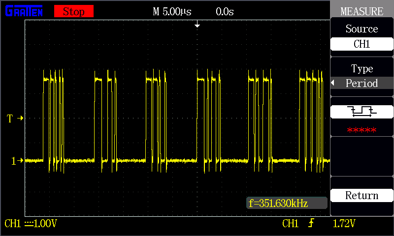
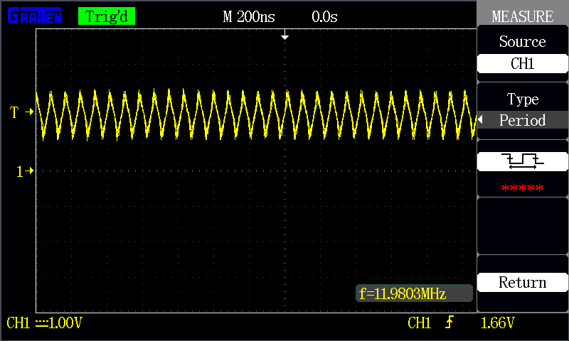
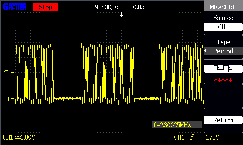
Any help you could provide would be appreciated! I've scoped out the signals and they appear to be what I expect (GPIO5 is outputting 24.576MHz). Just for kicks, I hooked up the BCK, DIN and LRCK signals, but register 91 reads 0x30, which indicates that the SCK is not a valid ratio of the sample clock.

Thank you

  • Hi Jonathan,

    Can you confirm the LRCK frequency as well? A scope shot of all 4 I2S lines to the PCM would be helpful.  

    I have attached an example config file you could look at. It should be pretty close to what you are doing with the exception that I have changed a few of the GPIOs. 

    PCM5122 GPIO PLL.TXT

    Please check your code against this.  The CP2114 is very similar to the device you are using.  And from a digital perspective, the PCM5122 is the same as the PCM5242.

    Thanks,

    Paul

  • Hi Paul,

    Thank you for the file, I'll take a look at that.

    In the meantime, here are some traces that may be useful. I can't get all 4 together right now, although if you need them all on the same capture, I can look at using my Saleae.

    DIN:

    LRCK:

    12MHz MCLK (into GPIO 6)

    GPIO 5 output (connected to SCK - Pin 26)

    BCK

    Thank you,

    Jonathan

  • Hi Jonathan, the clock ratios look okay, but I am a bit concerned about how the 24MHz clock looks.  Do you have a direct path from the GPIO to the SCK input? It is possible that you have too much capacitance on the line.

    Thanks,

    Paul

  • That's a good question, I will check this tonight. When you say you're worried about how it looks, what do you mean by that? I was looking at this last night, and realized that I hadn't grounded the probe especially well, so when I used the GND pin right next to the clock pin, the signal looked strong (i.e. higher peak-to-peak voltage). I also looked at it with just the probe attached (not jumpered back to the SCK), and it looked the same to me.

    Unfortunately on this hardware I don't have a way to directly connect the two, but I will likely do one more board rev and could add something better. If there are no other debugging steps that are useful to take, I can just do that and see if that fixes the issue, although that may take awhile.

  • Hi Jonathan,

    My concern is that peak-to-peak amplitude of the SCK is not large enough for the PCM to register it.  The voltages must comply with the VIH and VIL levels as specified in the datasheet.  A small series resistance may be enough to isolate the stray capacitance.

    Thanks,

    Paul 

  • Any updates?

  • Hello,

    Sorry for the delay -- I was out of town for the Thanksgiving holiday and am just getting back to looking at this now. Indeed it does appear to be related to the distance over which I was routing the clock lines. I did as you suggested and was able to "see" audio output on the output side of the chip. I imagine I'll have to re-think how I lay out the board to ensure that the clock signal is cleaner, but I have what I need for now.

    Thank you very much for the help!

    Jonathan