This thread has been locked.

If you have a related question, please click the "Ask a related question" button in the top right corner. The newly created question will be automatically linked to this question.

TLV320DAC3203: Drive Code for TLV320DAC3203IRGER

Part Number: TLV320DAC3203

Dear,

Where can I get the drive code for TLV320DAC3203IRGER, thanks a lot.

  • HI, Jiayu,

    I would suggest to take a look at this one: elixir.bootlin.com/.../tlv320aic32x4.c

    This is for the TLV320AIC32x4 and it is compatible with the TLV320DAC3203.

    Please let me know if you have additional questions or comments.

    Best regards,
    Luis Fernando Rodríguez S.

  • Hi Luis Fernando Rodríguez S.

    Thanks a lot.

  • Hi Luis Fernando Rodríguez S.

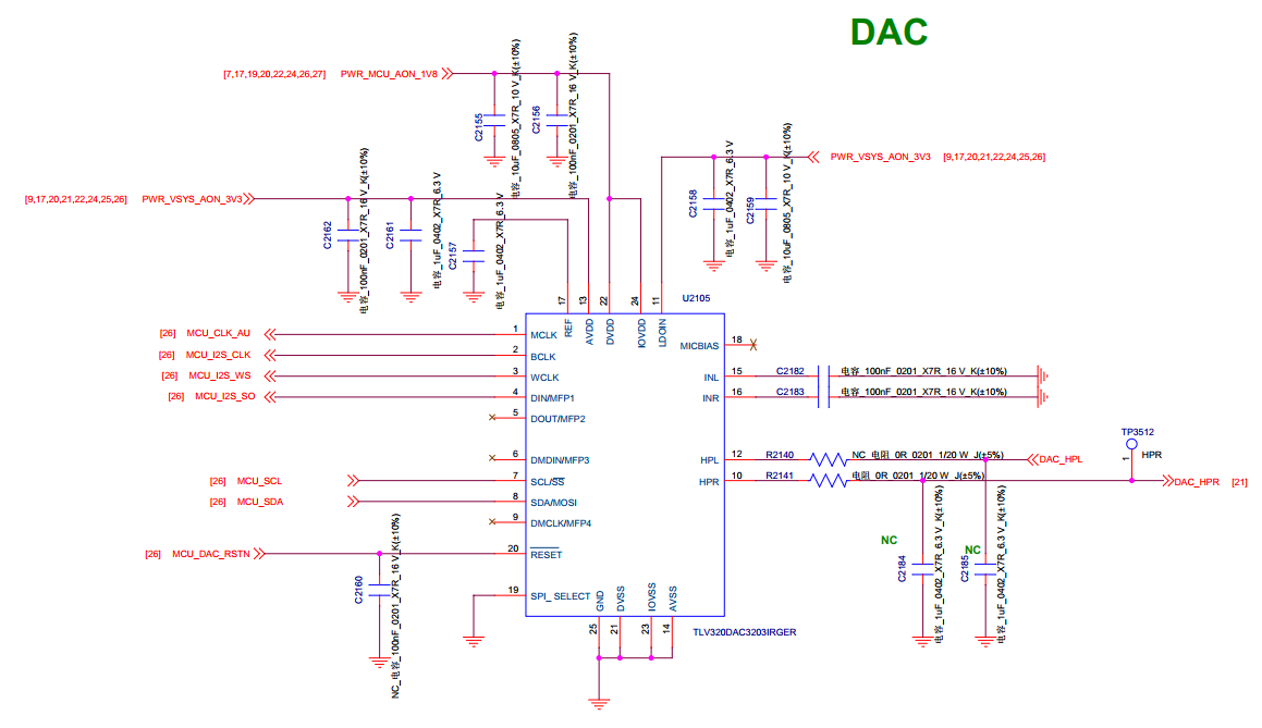
    (1) Below are the sch and block for this design. With TI codec TLV320DAC3203IRGER  and TI PA  TPA3111D1Q ,  do you have any comments or concerns for this design?

    (2) Actually, mono mode is used in this design, left channel of I2S audio data is sent from NXP DSP, so how to set the register for the TLV320DAC3203 to route the Left DAC to HPR

    (3) How to tuning to improve audio performance? Do we have reference code?

  • Hi, Jiayu,

    Thank you for providing the details about the circuit connections.

    I have few comments about the circuit, pleas take a look at the points below and let me know if you have further questions or comments.

    - I noticed that AVDD pin is connected to something that seems to be a 3.3V level. Is this correct or is it a typo in the diagram? The TLV320DAC3203 has a recommended power level of 1.5V to 1.95V. A power supply of 3.3V may even damage the device since AVDD absolute maximum range is 2.2V.

    - Also, since an audio DAC with integrated delta-sigma converter is being connected to an audio amplifier, we recommend to add a low-pass filter in order to remove the out-of-band content. Otherwise, there could be risk of amplifying also the out-of-band content. You may have more details about the suggested out-of-band filter in this document:

    https://www.ti.com/lit/an/slaa313a/slaa313a.pdf

    - The ground pins of the TLV320DAC3203 are all connected together. This is correct. However, in the PCB design, we recommend to separate the digital ground (DVSS, IOVSS) from the analog ground (AVSS, thermal pad) and connect both planes with single 0-ohm resistors or PCB traces. This will allow to reduce digital noise on the analog portion.

    - Regarding the TPA3111, I noticed SD and FAULT pins are not pulled-up to AVCC. As mentioned in the datasheet, both pins are voltage compliant to AVCC. So, I would suggest to pull them up to a AVCC through a 100K resistor.

    - Finally, I would suggest to move the capacitor C2164 and C2163 from the BSNx pins to the OUTx pins. You may find more details about the suggested connection in the figure 17 of the datasheet (https://www.ti.com/lit/ds/slos618f/slos618f.pdf#page=15).

    I will provide details about the I2C code in my following thread.

    Best regards,
    Luis Fernando Rodríguez S.

  • Hi, Jiayu,

    Please find attached a recommended registers configuration to route LDAC to HPR. This is the best performance configuration for the device.

    High_performance_mode_LDAC_to_HPR.txt
    ###############################################
    # High Performance Stereo Playback
    # ---------------------------------------------
    # PowerTune mode PTM_P3 is used for high
    # performance 16-bit audio. 
    #
    # Audio is routed to headphone outputs.
    ###############################################


    ###############################################
    # Software Reset
    ###############################################
    #
    # Select Page 0
    w 30 00 00
    #
    # Initialize the device through software reset
    w 30 01 01
    #
    ###############################################


    ###############################################
    # Clock Settings
    # ---------------------------------------------
    # The codec receives: MCLK = 11.2896 MHz,
    # BLCK = 2.8224 MHz, WCLK = 44.1 kHz
    ###############################################
    #
    # Select Page 0
    w 30 00 00
    #
    # NDAC = 1, MDAC = 2
    w 30 0b 81 82
    #
    ###############################################


    ###############################################
    # Signal Processing Settings
    ###############################################
    #
    # Select Page 0
    w 30 00 00
    #
    # Set the DAC Mode to PRB_P8
    w 30 3c 08
    #
    ###############################################


    ###############################################
    # Configure Power Supplies
    ###############################################
    #
    # Select Page 1
    w 30 00 01
    #
    # Disable weak AVDD to DVDD connection
    w 30 01 08
    #
    # Enable Master Analog Power Control
    w 30 02 00
    #
    # Set the input power-up time to 3.1ms
    w 30 47 32
    #
    # Set the REF charging time to 40ms
    w 30 7b 01
    #
    ###############################################


    ###############################################
    # Configure DAC Channel
    ###############################################
    #
    # Select Page 1
    w 30 00 01
    #
    # De-pop: 5 time constants, 6k resistance
    w 30 14 25
    #
    # Route LDAC to HPR
    w 30 0d 10
    #
    # Select Page 0
    w 30 00 00
    #
    # LDAC => 0dB
    w 30 41 00
    #
    # Power up LDAC
    w 30 3f 90
    #
    # Select Page 1
    w 30 00 01
    #
    # Unmute HPR driver, 0dB Gain
    w 30 11 00
    #
    # Power up HPR
    w 30 09 10
    #
    # Select Page 0
    w 30 00 00
    #
    # Unmute LDAC
    w 30 40 04
    #
    ###############################################

    Please let me know if you have additional questions or comments on this.

    Best regards,
    Luis Fernando Rodríguez S.