This thread has been locked.

If you have a related question, please click the "Ask a related question" button in the top right corner. The newly created question will be automatically linked to this question.

TLV320DAC3100: Registers settings for the TLV320DAC3100

Part Number: TLV320DAC3100
Hello,
I am trying to simply activate the I2S to output to the speakers.
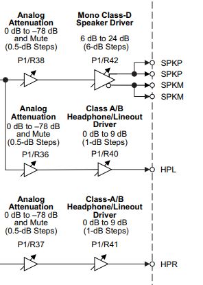
The chip has a lot of registers and I cannot figure out what registers I need to set in order to use is in I2S mode.
I am able to successfully talk to the chip using I2C and set the MICBIAS.
I am applying I2S signals to the chip and would like to know what registers I need to set in order to get outputs on the headphone and speaker.
1- On reset, which are the minimum registers setting I need to change in order to process the I2S input from my processor to output to the speaker. I am in desperate need to get the answer ASAP
Thank you
Miohammad Karaki

  • Hi, Mohammad,

    Welcome to E2E and thank you for your interest in our products!

    Please find attached a registers configuration script that you may use as a base for your registers configuration. You just need to ensure that the PLL and clock settings are correctly configured accordingly to the clocks you will be using in your application. This script contains the configuration for a MCLK = 11.2896MHz or 12.288MHz (which result in 44.1KHz and 48kHz sampling rate respectively). The BCLK and WCLK are configured as inputs in this script.

    2318.TLV320DAC3100_Script.txt
    # Key: w 30 XX YY ==> write to I2C address 0x30, to register 0xXX, data 0xYY
    # # ==> comment delimiter
    #
    # The following list gives an example sequence of items that must be executed in the time
    # between powering the # device up and reading data from the device. Note that there are
    # other valid sequences depending on which features are used.
    # 1. Define starting point:
    # (a) Power up applicable external hardware power supplies
    # (b) Set register page to 0
    #
    w 30 00 00
    #
    # (c) Initiate SW reset (PLL is powered off as part of reset)
    #
    w 30 01 01
    #
    # 2. Program clock settings
    # (a) Program PLL clock dividers P, J, D, R (if PLL is used)
    #
    # PLL_clkin = MCLK,codec_clkin = PLL_CLK
    w 30 04 03
    # J = 8
    w 30 06 08
    # D = 0000, D(13:8) = 0, D(7:0) = 0
    w 30 07 00 00
    #
    # (b) Power up PLL (if PLL is used)
    # PLL Power up, P = 1, R = 1
    #
    w 30 05 91
    #
    # (c) Program and power up NDAC
    #
    # NDAC is powered up and set to 8
    w 30 0B 88
    #
    # (d) Program and power up MDAC
    #
    # MDAC is powered up and set to 2
    w 30 0C 82
    #
    # (e) Program OSR value
    #
    # DOSR = 128, DOSR(9:8) = 0, DOSR(7:0) = 128
    w 30 0D 00 80
    #
    # (f) Program I2S word length if required (16, 20, 24, 32 bits)
    # and master mode (BCLK and WCLK are outputs)
    #
    # mode is i2s, wordlength is 16, slave mode
    w 30 1B 00
    # (g) Program the processing block to be used
    #
    # Select Processing Block PRB_P11
    w 30 3C 0B
    w 30 00 08
    w 30 01 04
    w 30 00 00
    #
    # (h) Miscellaneous page 0 controls
    #
    # DAC => volume control thru pin disable
    w 30 74 00
    # 3. Program analog blocks
    #
    # (a) Set register page to 1
    #
    w 30 00 01
    #
    # (b) Program common-mode voltage (defalut = 1.35 V)
    #
    w 30 1F 04
    #
    # (c) Program headphone-specific depop settings (in case headphone driver is used)
    #
    # De-pop, Power on = 800 ms, Step time = 4 ms
    w 30 21 4E
    #
    # (d) Program routing of DAC output to the output amplifier (headphone/lineout or speaker)
    #
    # LDAC routed to HPL out, RDAC routed to HPR out
    w 30 23 44
    #
    # (e) Unmute and set gain of output driver
    #
    # Unmute HPL, set gain = 0 db
    w 30 28 06
    # Unmute HPR, set gain = 0 dB
    w 30 29 06
    # Unmute Class-D, set gain = 18 dB
    w 30 2A 1C
    #
    # (f) Power up output drivers
    #
    # HPL and HPR powered up
    w 30 1F C2
    # Power-up Class-D driver
    w 30 20 86
    # Enable HPL output analog volume, set = -9 dB
    w 30 24 92
    # Enable HPR output analog volume, set = -9 dB
    w 30 25 92
    # Enable Class-D output analog volume, set = -9 dB
    w 30 26 92
    #
    # 4. Apply waiting time determined by the de-pop settings and the soft-stepping settings
    # of the driver gain or poll page 1 / register 63
    #
    # 5. Power up DAC
    # (a) Set register page to 0
    #
    w 30 00 00
    #
    # (b) Power up DAC channels and set digital gain
    #
    # Powerup DAC left and right channels (soft step enabled)
    w 30 3F D4
    #
    # DAC Left gain = -22 dB
    w 30 41 D4
    # DAC Right gain = -22 dB
    w 30 42 D4
    #
    # (c) Unmute digital volume control
    #
    # Unmute DAC left and right channels
    w 30 40 00

    Please let me know if you have additional questions or comments.

    Best regards,
    Luis Fernando Rodríguez S.

  • Hi Luis,

    The script is in the datasheet. It really sucks! I do not know who wrote it.

    I need to understand the chip reset mode, and what registers I need to set in order to simply accept I2S feed and output to the speakers.

    Thank you.

    Mohammad

  • Hi, Mohammad,

    In reset mode, all the registers are placed in default state (default state values specified on each of the registers).

    I prepared a new script with the minimum values you would require to route the I2S data to the speaker output. For a proper behavior, the I2S clocks must be configured as BCLK = 2.8224 MHz (or 3.072MHz) and WCLK = 44.1KHz (or 48KHz). The MCLK must be also provided for this example. MCLK = 11.2896 MHz (or 12.288MHz).

    TLV320DAC3100_I2S_SPK_44_1KHz_Script.txt
    # Commands format w 30 xx yy, where:
    # w is a write command
    # 30 is the I2C address in hex format
    # xx is the register address in hex format
    # yy is the register data in hex format
    #
    # Select page 0
    w 30 00 00
    # 
    # Software reset
    w 30 01 01
    #
    # Clock settings, MCLK = 11.2896 MHz, BCLK = 2.8224MHz, WCLK = 44.1KHz
    #
    # CODEC_CLKIN = MCLK, No PLL used
    w 30 04 00
    #
    # NDAC = 8, MDAC = 2
    w 30 0b 88 
    w 30 0c 82
    #
    # Left/Right channel DAC powered up and routed to left/right data
    w 30 3f d4
    #
    # Left/Right DAC not muted
    w 30 40 00
    #
    # Page 1 selected
    w 30 00 01
    #
    # Class-D Speaker amplifier powered up
    w 30 20 86
    # 
    # DAC channels routed to mixed amplifiers
    w 30 23 44
    # 
    # Class-D Speaker Amplifier unmuted
    w 30 2A 04

    Please let me know if it works for you or if you require additional support from our side.

    Best regards,
    Luis Fernando Rodríguez S.

  • Hi Luis,

    Good job. I see outputs now.

    However, I am confused about controlling the volume for the:

    1- Headphones, left and right channels

    2- The speaker

    Would you please give me the registers I need to use to adjust the volume?

    Thank you.

    Mohammad

  • Hi, Mohammad,

    I'm glad to read that you got good results with the script. Regarding the output gain, the registers associated to the volume are listed below:

    Speaker attenuation block (0.5dB steps): Page 1 / Register 38
    Speaker gain block (6dB steps): Page 1 / Register 42
    Left headphone attenuation block (0.5dB steps): Page 1 / Register 36
    Left headphone gain block (1dB steps): Page 1 / Register 40
    Right headphone attenuation block (0.5dB steps): Page 1 / Register 37
    Right headphone gain block (1dB steps): Page 1 / Register 41

    For more details, please consult the picture below:

    Best regards,
    Luis Fernando Rodríguez S.

  • Hi Luis,

    I am sorry. IT is still not working correctly.

    One more test to verify I am doing the right thing:

    The chip can generate a sine waveform. I tried to do that unsuccessfully.

    Do I need to provide MCLK in order to get the sine waveform?

    Thank you.

    Mohammad

  • Hi, Mohammad,

    This is correct, the TLV320DAC3100 requires of MCLK in order to generate the sine waveform from the beep generator. In addition, the beep can be only generated from the processing block PRB_P25. Do you have details about how you are configuring the TLV320DAC3100 to get the sine waveform?

    Thank you.

    Best regards,
    Luis Fernando Rodríguez S.

  • Hi Luis,

    Here is what I am using:

    /********************************************************
    example: Beep setting for a 1KHZ tone:
    Beep length = 0,0,0xf0
    SINE = 0x10B5
    COSINE = 0x7EE8
    ********************************************************/
    void GenerateSinWave(int channel, int frequency, int length)
    {

    SetPage(0);
    //----------------
    I2C.beginTransmission(TLV320Address);
    I2C.write(channel);
    //---------Beep length
    I2C.write(73);
    I2C.write(0);
    I2C.write(74);
    I2C.write(0);
    I2C.write(75);
    I2C.write(0xf0);
    //---------SINE
    I2C.write(76);
    I2C.write(0x10);
    I2C.write(77);
    I2C.write(0xB5);
    //---------COSINE
    I2C.write(78);
    I2C.write(0x7E);
    I2C.write(79);
    I2C.write(0xE8);
    //----------
    I2C.endTransmission();}

    Thank you.

    Mohammad

  • Here is the schematic I am using. Please let me know if you see any issues with it.

    Thank you

  • Hi, Mohammad,

    Thank you for providing the details about your testing and the schematic.

    Regarding the schematic, I don't see anything that should be modified. I would just suggest to remove the output capacitors C6 and C9. The speaker output doesn't require of them.

    Regarding the beep configuration, is it all the settings you are using? Do you have the rest of your code? Particularly, I don't see that the beep is being enabled by page 0 / register 71 / Bit D7. This is the bit that runs the beep.

    Best regards,
    Luis Fernando Rodríguez S.

  • Hi Luis,

    I did enable the register 71, bit 7 and still no output!

    I am getting frustrated since I tried your code, the sample code in the datasheet and tried to modify them without success.

    I am able to get MICBIAS to work which means the I2C interface is working.

    Here is the script I am using(where TLV320Address = 0x18):

    //********************************************************
    //********************************************************
    void I2C_SetRegister(byte reg, byte value)
    {
    I2C.beginTransmission(TLV320Address);
    I2C.write(reg);
    I2C.write(value);
    I2C.endTransmission();
    }

    //*********************************************************************
    //*********************************************************************
    void TLV320DAC3100_I2S_SPK_44_1KHz_Script()
    {
    //---page 0:
    I2C_SetRegister(0x00, 0x00); //set to page 0
    //---Reset
    I2C_SetRegister(0x01, 0x01);

    //Clock settings, MCLK = 11.2896 MHz, BCLK = 2.8224MHz, WCLK = 44.1KHz
    I2C_SetRegister(0x04, 0x00); //CODEC_CLKIN = MCLK, No PLL used
    I2C_SetRegister(0x0b, 0x88); //NDAC = 8
    I2C_SetRegister(0x0c, 0x82); //MDAC = 2

    //Left/Right channel DAC powered up and routed to left/right data
    I2C_SetRegister(0x3f, 0xd4);

    //Left/Right DAC not muted
    I2C_SetRegister(0x40, 0x00);

    //page 1 selected
    I2C_SetRegister(0x00, 0x01);

    //Class-D Speaker amplifier powered up
    I2C_SetRegister(0x20, 0x86);

    //DAC channels routed to mixed amplifiers
    I2C_SetRegister(0x23, 0x44);

    //Class-D Speaker Amplifier unmuted
    I2C_SetRegister(0x2A, 0x04);

    }

  • Hi, Mohammad,

    Do you select the processing block PRB_P25 in your registers settings? The Beep generation can be only done by this processing block (page 0 / register 0x3c / value 0x19).

    Best regards
    Luis Fernando Rodríguez S.