This thread has been locked.

If you have a related question, please click the "Ask a related question" button in the top right corner. The newly created question will be automatically linked to this question.

TLV320AIC3104: Input voltage levels for MIC2L, MIC2R and MIC1LP (SE)

Part Number: TLV320AIC3104

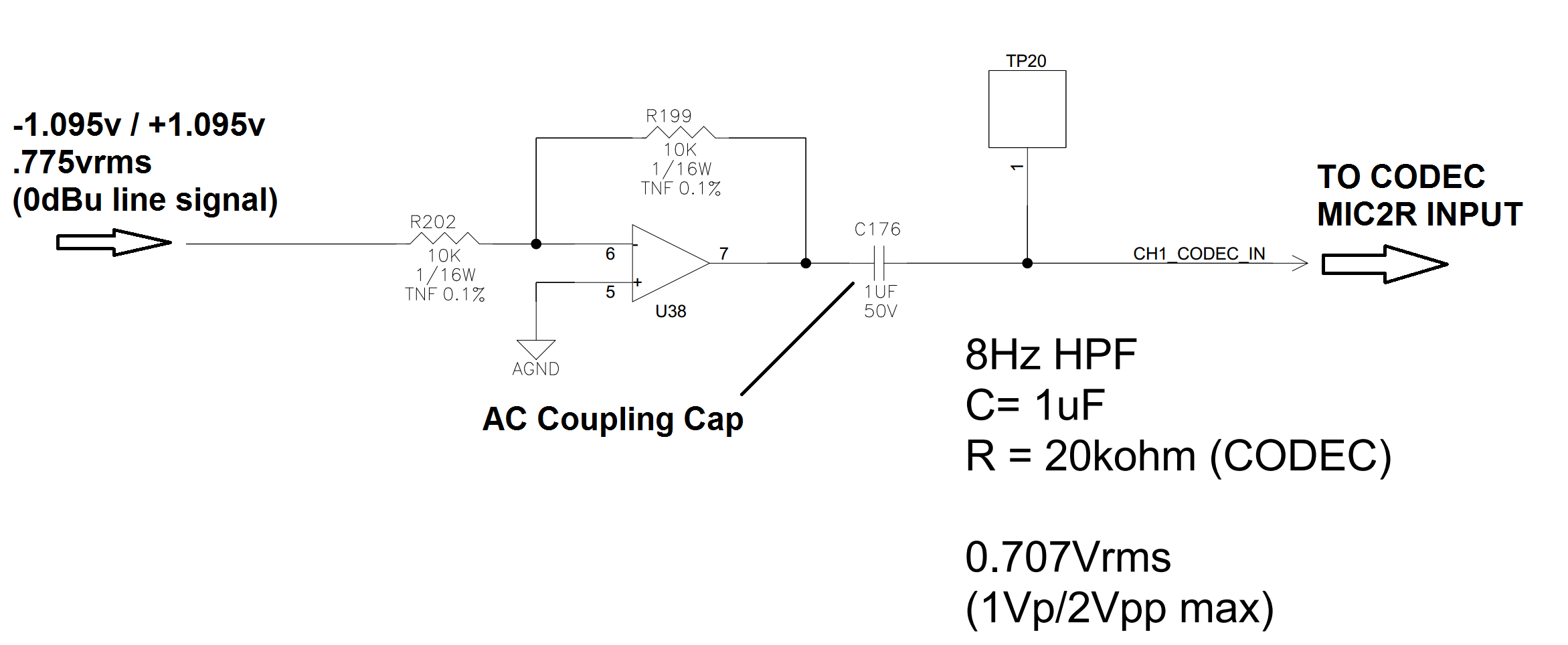
Per the datasheet, it indicates that the recommended level of inputs for these interfaces is 0.707Vrms.  However the absolute min indicates -0.3v and the absolute max is AVDD+0.3v.  We plan to inject a normal 0 dBu (pro audio signal) 0.775Vrms (-1.095v to +1.095v) line level signal, but this appears to be outside of the negative voltage range.  However, when probing the input pin of the codec with DC coupling mode the codec appears to apply a DC offset to bring the signal up to around 0v to 2.19v.  This would lead me to believe that the we are within the correct range. 

Do these inputs apply the DC offset as a constant level or does it change based on the input signal? 

Can you confirm this is using the codec correctly?

What are the maximum voltage ranges that can be applied to these interfaces?

Thanks!

  • Hi Gregory,

    If your input signal is AC coupled before the ADC, then the ~1.3V bias before the input stage of the ADC will bias the center of your AC waveform to that level and the application will work fine.  If you DC couple the input signal to the ADC then you will damage the device and violate the abs max specifications.  Any signal level shifting you're seeing with a DC coupled input is due to the input signal "fighting" the internal circuitry in the AIC3104 and is unadvised.

    Note that you will still need to slightly attenuate the input coming to the ADC or you will saturate the signal-chain as the max level is 0.707Vrms (+/-1Vpp), not including the typical non-zero gain error which is specified in the datasheet.

  • Thanks again Collin.

    The below image is a capture of the last stage before it connects directly to the codec.  We are using a 1uF (C176) AC coupling cap as indicated below.  The input to the final stage in our circuit leading up to the codec will be the +/-1.095v (0dBu line level) signal.  We will then apply some reduction to the input gain stage of the codec to make sure it doesn't clip since the codec is only expecting .707vrms.

    So just to confirm this method and circuitry is correct and will not damage the input of the codec?  Just want to confirm since we are not applying any DC bias to shift the signal up into the correct input range in our circuitry.  Is the ~1.3v DC bias supplied from the codec input stage a constant?

    Thanks!!  

  • Hello,

    That is correct, no damage will occur to the CODEC Inputs with this configuration assuming the output voltages of the amplifier remain within the ranges shown here.  If the amplifier glitches or shorts to the supply rails then larger voltages could temporarily make it through.

  • Thanks Collin.  Yea we noticed that on one of our boards due to an edge case transient.  We plan to add a clipper circuit to the left of the capacitor so that it will cap at no more than about +/- 1.2V.  thanks again for your help!