This thread has been locked.

If you have a related question, please click the "Ask a related question" button in the top right corner. The newly created question will be automatically linked to this question.

TPA3126D2: Output drops by 6dB

Part Number: TPA3126D2

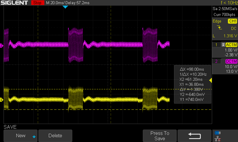
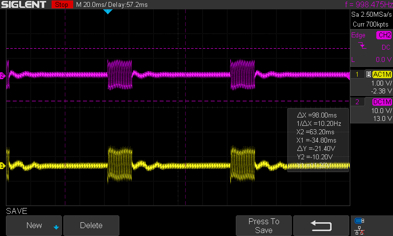
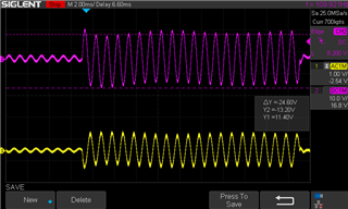
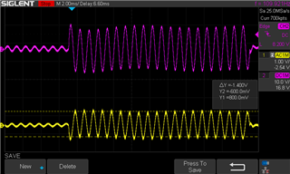
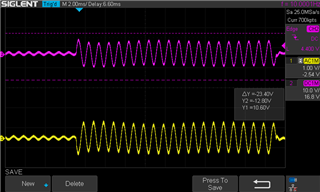
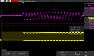
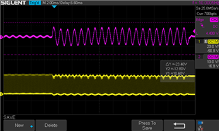
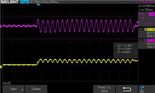
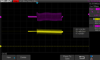
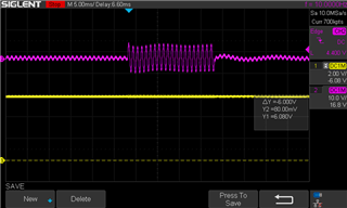
My design using the tpa3126d2 is showing an issue.  The output looks good but after playing a few minutes it drops by about 6dB.  Input voltages are the same.  Doesn't appear to be thermal related.  The audio input signal is at the same level.  The input is single ended.  Checked the GVDD voltage and see no change when the level drops.  Any ideas?

  • Hi,

    Could you please share your schematic to us? You attached picture can not be shown.

    One question, did the output power reduce slowly or quickly when reach one power point?

    Regards,

    Derek

  • Hi,

    Did you check power before common choke (after LC filter)?

    TPA3126 output will reduce slowly on high power since of thermal, but the power reduce will be very slowly and very low.

    I am afraid that the peripheral circuit will have influence.

    And you can also check on EVM board.

    Regards,

    Derek 

  • There doesn't appear to be any drop on the common mode choke.  Additionally, this is a configuration for this part I've used on a couple other designs and have not ran into this issue.  The drop in output is a definite step change, and stays constant after no longer how long I stream signal.  I've seen thermal cycling before, and the fault line triggers and the amp goes into total shut down, during that case.  The amp is running off of a 24V PVCC rail.  Before the fold back, I'm getting about 28Vp-p into a 4 ohm load.  After the fold back I'm getting about 14Vp-p.

  • Hi 

    What's the test point? Did you check on EVM board yet? 

    Regards,

    Derek

  • I don't know what "test point" you refer to.  If you mean where am I taking my voltage measurements at, I'm comparing input voltages at the input cap to the amp, and the output voltages across the 4 ohm load.  I did check, as you requested, the input voltage to the common mode choke in the output emi filter, but it was the same as the voltage across the load during this "fold back" condition.  I'm not sure what the evaluation board would have to do with this at all since its different circuitry.

    As I mentioned before, this is my 4th implementation of this same output configuration.  I have not seen this issue before.  So yesterday I was able to have some thermal images done comparing this design to one of the previous implementations.

     This shows a the max temperature of a similar implementation of the chip without the heatsink .

    This shows the new design in the same condition (without heatsink) just prior to the gain reduction .

    And this shows the new design after the gain reduction

    In comparing the two layouts the only difference is that the first design has vias under the chip.  The new design has them removed because we were/are fighting emi issues and I was told that stitching the ground planes together can cause worse emi than not.  Obviously this is telling me that the thermal conduction of those missing vias is needed, and that our heat sink design is not performing as required.  According the the spec sheet on this part, I should be able to run 50W continuous though this amp chip, and yet I have not been able to do that without going into full thermal cycling which I now believe is due to the heat sink design not properly keeping the chip temperature down, which is what I always believed but have not actually required to run it at 50W yet.  What I don't understand is why this doesn't go into a fault condition due to thermal, but instead seems to fold back about 3dB based on actual voltage calculations, then stabilize.   I had pictured the thermal protection to be (and witnessed this function as) more of a step condition.  Violate the temperature and the chip shuts down, will restart after a time delay due to how we've connected the SDZ line to the FAULT line.  I've ordered some freeze spray and will attempt to cool the chip to see if the gain corrects itself, but I'd like to understand exactly what I should expect from a over temperature condition.

  • Hi,

    Thanks for your clear description!

    I can't believe that thermal vias under chip can affect EMI performance. I think the vias can not affect EMI. The thermal vias under chip is very important for thermal, if you can add enough vias under chip, it will have great help for thermal.

    Device internal Rdson impedance will increase with thermal, so on high power, the power dissipation will increase quickly if bad thermal design.

    I think the fault is OTSD fault when high power.

    Regards,

    Derek 

  • So that was my first thought also.  I obtained some freeze spray and after the part reduced its output level, I applied the coolant.  The part did not recover.  So my questions are:

    1. If this is thermal, why does the part not pull its FAULTZ line low?
    2. Are there thermal conditions that would require a power reset to recover from?

    On additional test I ran was that while operating in what we believe is this thermal condition, I manually pulled the FAULTZ line low (which is tied to the SDZ line), while applying the freeze spray.  When I released the line, the amp performed with the proper gain (until it heated up again of course).  This would imply that there is a thermal condition that does not actually activate the fault line.

    Thoughts?

  • Hi 

    The OTSD fault is latched, it can not be auto-recover.

    The only thing I can thought is OT issue. Could you check on EVM board with same condition?

    Regards,

    Derek

  • First how can I duplicate this apparent thermal issue on the dev board?  Second, if its an OTSD fault, why is the FAULTZ line not being pulled low?  Lastly, the FAULTZ line is tied to the SDZ line so that, based on my understanding and testing, it will reset the fault latch.   So the main issue I see is why is the FAULTZ line not being pulled low if there's a thermal fault?  Also I didn't get email notification that  you replied, so sorry for the late response.

  • Hi,

    I mean the thermal lead to internal Rdson impedance increase quickly in short time. The higher temperature, the higher Rdson impedance. That will lead to output power reduce. with thermal reach to OTSD point, OTSD fault will be triggered, and fault pin will be pull-low.

    According to your comparison with old board, the issue board has thermal problem, so internal Rdson impedance is more higher than old board. Then output power is lower. That makes sense.

    You can input same audio input level and check output power on EVM board.

    Regards,

    Derek

  • I'll try to check, but the Fault line is not being pulled low.  This is on multiple assemblies, so its not a one off.  Why is the fault line not being triggered?

  • Hi 

    If fault pin is not pull-low, it is not OTSD fault. That means temperature did not reach to OTSD threshold.

    Regards,

    Derek

  • Ok, then why is the output power dropping, or is there an area of heating that will drop the output power by 3-6dB without a over temperature error?  I find it odd that the board reacts the same with or without the heatsink attached.  The heatsink is the same as the TI design on the EV board.

  • Hi,

    With device thermal temperature, device internal Rdson will increase. So the resistance Rdson consumes more power. That lead to output power reduce.

    Regards,

    Derek

  • So you are saying that the power output will start to drop as the chip heats up from the start, and then the fault line is exerted when it finally heats enough to hit the over temperature limit point?  Is this somehow specified in the speck sheet for the part?

  • Hello 

    There isn't a datasheet spec for the Rdson vs temperature. In our datasheet we do provide information for the thermal protection limitations.

    Best regards,

    Luis

  • You didn't answer my question, so let me ask it differently.  If I program the part for lets say 26dB gain, now much of a gain reduction should I expect BEFORE it hits the thermal limit?  From what you are saying there is a range between a totally cool part, and the thermal protection activating and pulling the fault line low.  I'm seeing at least a 3-6dB drop potential since the parts I have are not pulling the fault line low, but obviously thermally folding back.  So from a design standpoint, exactly HOW do I design to achieve a specific gain?

  • Hi,

    Thermal make output power reduce, but thermal could not trigger fault pin to low if thermal is not very tough.

  • I'm sorry, I would not expect a 3-6dB drop in output power before the thermal protection kicked in.  That seems like something that should be covered in the spec sheet.  I'm still waiting for the new boards to prove that the issue is indeed fixed with the addition of the vias under the part.

  • Hi,

    That's good idea.

    Waiting your feedback.

    Thanks!

  • Hi,

    I am thinking that if device Gain setting is error. You set to 26dB Gain, but device turn to 20dB when something error. 

    Did you find the Fault pin pull to low before output drop 6dB?

  • No the fault pin never went low.  The audio just folded back after the device hit some internal threshold (assuming thermal).  If the fault pin had activated I would have understood the issue, but no it never did.

  • So the vias under the amplifier chip did not solve the issue, though they do help the chip run a bit cooler.

     So in running the part (note this is without the heatsink, though the same thing happens with the heatsink, I get the following in a cool state:

    The top trace is the amplifier output at the 4ohm load, the bottom trace is the signal into the amplifier. I’m getting roughly 12V peaks at the load, with an ~ 1.35V P-P input signal as shown below.

    When the unit goes into this fold back condition I get the following with roughly 6.5-7V peaks (roughly a 4-5dB drop):

    While the input voltage remains the same.

    I’ve checked the voltage at pin 8 (Gain/SLV) and it does not change, and as you can see from the previously pasted schematic, PLimit is tied to GVDD thus disabled. PVCC remains constant at 24.8VDC. 

    I need some help on this, and its became urgent. This is for one of our biggest customers and we're now impacting the project timeline.

  • Ok, here's another interesting phenomenon.   

    I switched my AP from the burst to a constant sine wave and reduced the level.  I'm getting about 9Vp (and remember as in the previous post, these signals are on both right and left channels and again without the heat sink) at the load. 

    The device is going in and out of thermal shut down (fault/SDZ low) am recovering in about a second.  About one out of 10 times, when the unit returns at the lower gain.  This may or may not be related.  The next cycle the unit returns to the proper output. 

    Again, the continual cycling is due to the fault line being tied to the SDZ line clearing the fault.  In the burst testing, the unit remains in the low output state until the fault/SDZ line is take low and return, so this is some sort of latching state, but the fault line is not being taken low.

  • Hi,

    When device power up, device will sample Gain/SLV pin voltage to latch the Gain setting. And the Gain/SLV voltage is divided from GVDD using resistors.

    Usually SDZ and Fault pin are connected together, when fault happen, fault pin will pull to low, then SDZ will pull to low and restart device. Then device will re-sample Gain/SLV pin voltage to latch the Gain setting again. 

    So I suggest you can monitor the Gain/SLV pin voltage to compare the difference of good and issue cases. Please test the voltage on pin side as possible.

  • As I've already reported, the voltage on the Gain/SLV pin does not change.  Device powers up with the correct gain, then later is reduced, but the pin has the same voltage on it.  Again, the Fault pin IS tied to the SDZ line for automatic reset of fault conditions.  And the PLIMIT pin is tied to GVDD so there is not additional power limitation.

  • Hi,

    The device will latch the Gain setting when power up and will re-latch when toggle SDZ.

    I suggest you should monitor SDZ, Gain/SLV and output waveform together using oscilloscope.

    Otherwise I did not find out other points. Because I do not have your boards in hand, and I also can not reproduce on EVM board.

    Can you ask TI FAE to onsite support?  And can you check on EVM board?

    I think FAE onsite support should have more effect. 

  • I did monitor the Fault line and the Gain pin with a scope, and there was no changes.  If the Fault line is not being pulled low, how could a new value be latched in?  As for TI support, I have no clue as to who the FAE is for Portland Oregon, and have pretty much been told that these forums are our only line of support, and I'm not finding that very supportive.

    Can you escalate this to someone else? 

  • Hi,

    Does the issue happen on some devices or all devices? Do you have EVM demo board in your hand?

    When device power up, it will sample the Gain/SLV pin voltage again. But you said the Gain/SLV pin voltage did not change, so the Gain setting will be not changed. 

    According to your description, I can not find out other possible points. So I suggest you can check on EVM board if you do not have FAE support.

    As you know, sometimes HW debug needs board in hand, but I do not have your board. I also meet this issue before.

    You said you have old board that has no this issue, right? Which the differences except vias under device? Compare the difference in detail may be best way.

    I am sorry for that!

  • I feel this is a very cyclical conversation and we've covered all this information already.  Once again:

    1)  This issue is happening on every one of this latest design.  The 4 previous boards I had made, then the two so far I've brought up of the 4 new boards I had made with the thermal vias added under the amp chip.  I have three other designs all using this same amp chip, one of which is in production, and two are going through validation testing now.  I did not encounter this issue on those designs.  The amplifier output configuration and set up is pretty much the same on all 4 designs, with the differences being in the signal chain prior to the chip.

    2) Eval board:  Yes I have one, but I have not wired the design outputs of this current design into it, what would be the point, since as I have just stated, I have implemented this chip design several times before and not seen this.

    3) The reduction appears to be thermal, though the fault pin is NOT being activated.  I can actually get the board into this reduced state, hold the fault pin low, cool the chip constantly with freeze spray, and while cooling release the fault line.  The part works correctly until I stop applying the freeze spray, the the output will reduce (note that the Fault pin is still not activating).

    Yes I know hardware issues are hard to diagnose, though these are very specific symptoms outside the data sheet.  I entered a help ticket with TI and will see what other information I can get.

  • Hi,

    Got it! Thanks!

    Thermal do reduce output, but output reduce is very slowly.   6dB reduce is crazy...

    Did you check PVCC power supply when issue happened? Please check if PVCC reduce when high power output, then it will make output power reduce.

    If 4 designs schematic designs are same, I think the points may be PCB layout.

    You can also move one issue device on EVM board to double check.


  • Hi,

    Yes, I checked the PVCC supply, and its steady at ~24VDC.  I can't see anything on the layout (which I shot a copy of the amp chip portion) that would cause this.  While none of the boards are identical, there isn't much difference regarding the amp.

    I don't understand what you mean regarding "You can also move one issue device on EVM board to double check."?

    Thanks,

    Michael

  • Hi,

    I mean that you can take off one device which is on issue board, and mount the IC on EVM board to double check.


  • First for the record, this issue is not resolved, nor have I heard anything back yet form the help case that has been entered.  I'm not about to remove ICs from the dev board and put them on these target boards fearing to make my dev board inoperative.  That being said, I did have one part that had a non related issue (short on the chip output) that was either a solder bridge under the part, or a bad output on that part.  I did replace it with parts I had gotten over a year ago left over from a build on a different project.  That did not fix the issue.  Its interesting that if I back the input signal off a couple of clicks, the part will run continuously (without heat sink), with about 10 volt peaks.  This is even after the part got into the odd fold back condition, and I reduced the input signal, and reset the fault line, so the part would be starting at about the same temperature.

    I've no idea where to go next. 

  • Hi,

     Its interesting that if I back the input signal off a couple of clicks, the part will run continuously (without heat sink), with about 10 volt peaks.  This is even after the part got into the odd fold back condition, and I reduced the input signal, and reset the fault line, so the part would be starting at about the same temperature.

    I can not understand what you mean. Did you compare the good board and issue board, including PCB and schematic?

  • Is there any way we can escalate this issue to either another customer service tech or a manager? Our company has been trying to solve this issue for two months. We need to find a resolution to this problem.

  • Hi

    Could you share you PCB layout and schematic to me? Let me check it.

    And did you check each pin voltage and waveform, compared good board and issue board?

  • The previous comment was from my boss and we've already shared all the specifics of this issue (schematic, layout).  I've entered an official help ticket, but they apparently are unable to help and sent me back to these forums.  TI is apparently unable to answer simple questions regarding their product such as is the gain setting of the chip affected by the input signal?  In other words if the gain is set to 26dB, does it change from that value when going to single ended inputs, or does the chip automatically adjust the gain based on input configuration.  Again, you have marked this thread as "thought resolved" where in fact TI has yet to provide guidance to resolution of this issue.

  • Hello,

    I would encourage you to find a local TI support. An onsite support may will helps resolve this issue more efficiently.  In this E2E forum, we have quite limited information exchange and limited resource to help you effectively.

    Still, we would like to analysis the issue more logically. so, please help do below.  

    1. Please capture PVCC waveform.(after filter inductor)

    2. Please capture audio input waveform before input cap.

    3. Please capture OUTP and OUTN PWM waveform.

    4. Please capture waveform right after LC filter, both P and N

    5. please capture  PLIMIT waveform

    Dylan

  • If you have actually followed this thread, you would see that most the things you've requested have already been provided.  As to the PLIMIT "waveform" it is tied to GVDD and is constant.   And I've asked who I could reach out to locally, but still have not been given an answer to that question along with several other questions.  Here is the summary that I've been requested to provide:

    The issue I’m having in this design is that the chip will power up with one gain, then some time later (minutes if cold) the gain drops by 4-6dB while the input signal remains constant.  The fault line never gets activated to indicate some fault (thermal, current, etc).  The gain just drops.  The issue does appear to be thermal related and the condition does appear to be latched.  When in this “thermal foldback” condition, I can manually pull the fault line low, apply freeze spray, and the condition does not re-occur until I stop applying the freeze spray.  Then it returns.

    This reduced output condition is also stable.  In other words it has not been observed to continue to reduce output.  In fact, I can increase the signal being fed to the amp and it will increase the output without further reduction. 

    I’ve asked the question several times, but not received a reply, about what the gain “should” be.  The signal to the amp is set in hardware to be 26dB.  The signal is single ended, not differential, so I figured that my gain would be reduced 6dB.  In the “non-foldback” condition, the gain is closer to 26dB, and then gets reduced to closer to what I expected (20dB).  In trouble shooting this, I noticed that the demo board provides a consistent 26dB in single ended.  So what gain should I see?  Does the chip compensate gain for input configuration, or is the gain setting for single ended and I would need to add 6dB if I went to differential input?

    Things I’ve tried:

    • Compared operation to other designs I’ve done and they don’t exhibit this same gain reduction, though at one point, I did force one of the other designs into a thermal cycle condition (Over temperature pulling fault low, resets because fault line is tied to the SDZ line) and noticed the first 2-4 cycles of the 1KHz input signal I was sending was at 26dB, then reduced to 20dB, so this could be happening on other designs, just too fast to be noticed.
    • Removed the amp chip on one of the samples of the design with the major issue, and replaced it with a sample of the part I had left over from one of my earlier projects using this chip (maybe a year an a half ago). The problem remained the same.
    • Hooked up the demo board to the design to the PVCC supply of the design in question and it does not appear to exhibit this issue.
    • Removed the common mode choke on the output (common configuration on the last 3 of the 4 designs I’ve implemented using this part) and that did not correct the issue.
    • Removed the ground on the capacitor feeding the negative input side, and ran it back to the ground pin on the op amp feeding the signal. No effect.
    • Tried changing the chip oscillator frequency from 1.2MHz to 400KHz, but no effect.
  • Hello,

    To help solve the issue your have, please provide enough information, so we can do the analysis systematically.

    I believe there was some misleading information during communication before, One example is PLIMIT is in fact not directly connected to GVDD.(if i understand correctly the schematic your provided). And actually i only see one waveform of output, not all the information.  So, we need you provide the waveform captured during issue happen.

    1. Please capture PVCC waveform.(after filter inductor)

    2. Please capture audio input waveform before input cap.

    3. Please capture OUTP and OUTN PWM waveform.

    4. Please capture waveform right after LC filter, both P and N

    5. please capture  PLIMIT waveform

    Again, I would encourage you to find local TI support. Online communication has many restrictions, and could have misleading communication, which is not helpful to resolve your problem effectively.  You can find TI local support from distributor.

    Dylan

  • So first, why is it no one at TI has answered my question about the expected gain?  You also say I should reach out to local TI support, yet no one from TI has provided the information of who or how I can do that?  Your web site is a joke when it comes to locating support.

    The audio input signal waveform has previously been provided above in both pre and error states.  In fact, the wave form is the same (outside of DC bias) on both sides of the input cap during the error condition.  I will endeavor to redo the other waveforms you have requested. I'm assuming since you want the OUTP and OUTN PWM waveforms referenced to GND (or common)?  And the wave form "right after" the LC waveform is before the common mode choke.  Also, the PLIMIT is tied to GVDD through a zero ohm resistor and I have, in fact, removed that zero ohm and replaced it with a direct short, but there was no change in the operation.  Besides, since the Fault is not being pulled low, the PLIMIT and Gain should already be set from the initial power up correct?  

  • Upper Trace measured (Waveform pre fold back @ 4Ohm load).

    Bottom Trace input signal.

    This next image is a repeat from above only measuring the input waveform.

    Again: Non Foldback condition, top trace at load, bottom input signal measured

    Fig 3: Top trace, Foldback condition at load, Bottom Trace input signal.

    All the above input signals are taken on the input side of the coupling cap to the chip.

    These next waveforms are all in the fold back condition and are what I believe you've asked for.

    OUTPR

    OUTNR

    Output from LC filter P

    Output from LC filter N

    PVCC @ Chip

    PLIMIT Pin

    Note: These last two images I moved the measurement cursors to the yellow trace (actual measured information) to allow more accurate measurement of those signals.

    If there's some different images of these waveforms you need please let me know.  Also, please answer my questions.

  • Hi,

    I am sorry the issue was not fixed till now. 

    Do you use same Bom on good board and issue board?  To debug, I suggest you can simplify the design. Use external PVDD power with sufficient current ability. And remove common coke, only keep LC filter on output. 

    I am sorry that I do not know how to contract to local FAE to support you. Let me check it.

  • I'm sorry, "fixed till now"?  Not sure what you mean?  The issue is still not fixed, nor have you answered my question about gain.  As for your questions, I have ran the PVDD supply from the board with the issue into the demo board and the problem did not exhibit itself on the demo board.  I took a board that had the issue and removed the common mode choke.  That did not have any effect.  Any other thoughts?

  • Hi,

    From the waveform, the output seems clipping, over PVCC. Did you try to reduce audio input level and double check?

  • These waveforms (as stated) were taken with the device in the reduced gain state.  There is no clipping in either state in any case.

  • So let me ask you.  Exactly WHY are you not answering my question regarding gain?  Do you simply not know?  If that is the case, is there no one within TI to ask?  I'm puzzled as to why I can't get this answered, and in fact I now believe it goes to the heart of the issue, and exists in other parts you have that are based on this same configuration.  I did swap out the amp chip on one board with the TPA3156 which appears to be basically the same part, but with higher power handling capability.  It did the EXACT same thing.  So I took one of the boards with the issue, and reduced the gain to the parts minimum 20dB gain, and boosted the input signal by 6dB to keep the signal chain gain to the same over all point.  The part no longer reduces its gain, and continually puts out the same output signal as seen previously BEFORE the gain reduction.  So tell me, this pretty much eliminates everything else being the issue, does it not?  I need to understand what is happening here or I won't be able to use these parts in any future designs.  

  • Hi,

    So you mean you replaced on TPA3156 device on issue board, it can work well, right?

    From your first picture, the output Vpp is 24V, and your power PVCC is also 24V, so I think the output was clipping firstly. 

    What's the load and output power of your application? TPA3126 can support to 50W at 4ohm load. If you need to drive higher power, I suggest you can select TPA3156 which can support to 70W.