This thread has been locked.

If you have a related question, please click the "Ask a related question" button in the top right corner. The newly created question will be automatically linked to this question.

TLV320AIC34: Signals sign and Digital effect filters

Part Number: TLV320AIC34
Other Parts Discussed in Thread: REG101, REG102, REG103, REG104

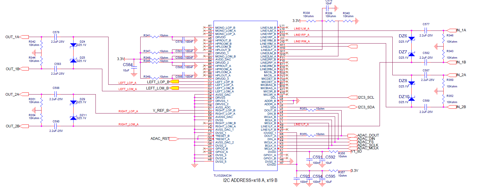
On my board I have the CODEC TLV320AIC34 for stereo audio interface (A section) and to generate constant polarization signals (B section), 16KHz sampling rate, DSP interface.

  • I have noticed a sign inversion on the output of signals LEFT_LOP_B/LEFT_LOM_B: when I send a positive value (16bit: 0x2000) on the DIN interface I would expect LEFT_LOP_B> LEFT_LOM_B actually LEFT_LOM_B> LEFT_LOP_B and vice versa when I write a negative value (16bit: 0xe000). Am I doing something wrong?
  • In case of a single ended output, can I use only one RIGHT_LOP_B output and leave the LEFT_LOM_B output floating?
  • In the DAC section, I use DAC_L3 connected to LEFT_LOP_A / LEFT_LOM_A and DAC_R3 connected to RIGHT_LOP_A / RIGHT_LOM_A. How can I enable digital effects filters in the DAC section? Is it enough to set the coefficients on page 1 or there is some registers on page 0?

Thanks

Francesco

  • Hello Francesco,

    Apologies for the delayed response.

    Let me check this in the lab and will get back to you as soon as possible.

    Regards,

    Aaron

  • Hello Francesco,

    To answer your questions:

    • I tested this in the lab and did not see any unexpected results. I applied a clipped sine wave using Audacity and recorded the Left/Right_LOP/M_B outputs. All the outputs were in phase and the LOM channels are inverted. Do you have any scope shots/schematics you can share? 

    • Yes you can leave the output floating. This is not an issue. 
    • Register 12 on Page 0 is where you enable Digital Effects and Page 1 is where you set the Digital Effects Filter coefficients. 

    Regards,

    Aaron

  • Dear Aaron,

    thanks for your answers.

    About my first question, probably, I wasn't clear.

    In the picture below I show DIN (4 channels, 16bit, CODEC_A with Reg10: 0x00: Data offset = 0 bit, CODEC_B with Reg10: 0x20: Data offset = 32 bit). On CODEC_B, left and right channels, I send a fixed value: -16384 (0xC000). Output common-mode voltage = 1.8 V (Reg.40 (D7-D6) = 11)

    With a negative value (-16384), I have LEFT_LOP_B > LEFT_LOM_B. 

    I would expect LEFT_LOM_B (minus) > LEFT_LOP_B (plus).

    What am I doing wrong?

    Regards

    Francesco

  • Hello Francesco,

    I don't quite understand how you are measuring the outputs. I see CH.3 cursors but looks like you might be trying to measure CH. 4? Can you clarify what voltage level you are seeing on the two outputs? It looks like you are measuring ~2.5V on CH.3 but I am unsure on CH.4.

    Are you using an EVM? If not, a schematic if your circuit would be helpful.

    Regards,

    Aaron

  • Hello Aaron,

    CH.3 is 2.4V and CH.4 is 1.26V (cursor a). Common-mode voltage = 1.8 V (cursor b). I have two probes with GND as reference. CH3 marker is over CH4, so you can't see CH.4. 

    In yellow LEFT_LOP_B and LEFT_LOM_B.

    Below the schematics:

  • Hi Francesco,

    Thanks for the detailed info and the schematic. 

    What is going on in the LINE2LP/M_A inputs? What is the purpose for feeding a known DC voltage in the input? Could you also please share your register configs for the device? 

    Regards,
    Aaron

  • Hi Aaron,

    LINE2LP/M_A inputs are intended for HW version definition: resistors change depending on HW version of the board.

    Below you can find the file configuration registers (VHDL).


    Regards

    Francesco

    -- MCLK = 12 MHz and fS(ref) = 48 kHz
    -- P = 1, R = 1, K = 8.192, which results in J = 8, D = 1920
    -- fS = 16 kHz, fS(ref) = 48 kHz, and the DAC fS set to fS(ref)/3.


    constant LUNG_INIT_CODEC : integer := 110;  -- 1 Address + 109 registers
    type Initial_codec_A is array (LUNG_INIT_CODEC-1 downto 0) of std_logic_vector (7 downto 0);

    ---- CODEC A ---------------------------------------------------------------------------------------------------------------------

    constant Initial_codec_A_const : Initial_codec_A:= (
       "00000001",  -- Starting Address
       "10000000",  -- Reg1: SW RESET
       "01000100",  -- Reg2: 0100: ADC fS = fS(ref)/3, 0100: DAC fS = fS(ref)/3 = 16KHz
       "10100001",  -- Reg3: 1: PLL is enabled, 0100: Q = 2, 001: P = 1

       "00100000", -- Reg4: 001000: J = 8, 00: reserved
       "00011110", -- Reg5: 00011110: PLL D value – Eight most-significant bits of a 14-bit unsigned integer
       "00000000", -- Reg6: 000000:PLL D value – Six least-significant bits of a 14-bit unsigned integer, 00: Reserved. Write only zeros to these bits.
       "00001010", -- Reg7: "000", 01: Left-DAC data path plays left-channel input data, 01: Right-DAC data path plays right-channel input data,
       "00100000", -- Reg8:
    --  ||||||++------ 00: Digital microphone support is disabled.
    --  |||||+-------- 0: Disable 3-D digital effect processing.
    --  ||||+--------- 0: Reserved
    --  |||+---------- 0: BCLK_x (or GPIO2_x if programmed as BCLK_x) / WCLK_x (or GPIO1_x if programmed as
    --  |||               WCLK_x) does not continue to be transmitted when running in master mode if codec is powered down.
    --  ||+----------- 1: Place DOUT_x in high-impedance state when valid data is not being sent.
    --  |+------------ 0: WCLK_x (or GPIO1_x if programmed as WCLK_x) is an input (slave mode).
    --  +------------- 0: BCLK_x (or GPIO2_x if programmed as BCLK_x) is an input (slave mode).
       "01001110", -- Reg9: 01: Serial data bus uses DSP mode, 00: Audio data word length = 16 bits
                    -- 1: 256-clock transfer mode used, resulting in 256 bit clocks per frame,
                    -- 1: Re-sync stereo DAC with codec interface if the group delay changes by more than ±DAC (fS/4).,
                    -- 1: Re-sync stereo ADC with codec interface if the group delay changes by more than ±ADC (fS/4).
                    -- 0: Re-sync is done by internally soft-muting the channel. (ADC/DAC)
       "00000000", -- Reg10: 00000000: Data offset = 0 bit clocks. MSB bit dopo un clock dal FS (WCLK_x)
       "00000001", -- Reg11: D3-D0=0001 : PLL R Value = 1
       "00000000", -- Reg12: High-pass, digital effects, De-Enphasis Disabled
       "00000000", -- Reg13: Headset or Button Press Detection Register A Disabled
       "00000000", -- Reg14: Headset or Button Press Detection Register B Disabled
       "00000000", -- Reg15: 1: The left-ADC PGA is muted., 0 gain Left-ADC PGA Gain Setting
       "00000000", -- Reg16: 1: The right-ADC PGA is muted., 0 gain right-ADC PGA Gain Setting
       "11111111", -- Reg17: 1111: MIC3L_x is not connected to the left-ADC PGA., 1111: MIC3R_x is not connected to the left-ADC PGA.
       "11111111", -- Reg18: 1111: MIC3L_x is not connected to the right-ADC PGA., 1111: MIC3R_x is not connected to the right-ADC PGA.
       "10000111", -- Reg19: 1: LINE1Lx, LINE1LP_x is configured in fully differential mode. LEFT ch.
                    -- 0000: Input level control gain = 0 dB
                    -- 1: Left-ADC channel is powered up.
                    -- 10–11: Left-ADC PGA soft-stepping is disabled
       "11111000", -- Reg20: 1: LINE2L is configured in fully differential mode. LEFT ch.
                    -- 1111: LINE2L is not connected to the left-ADC PGA
                    -- 0: Left-ADC channel is powered up.
                    -- 00: Reserved. Write only zeros to these register bits.
       "11111000", -- Reg21: 1: LINE1R is configured in fully differential mode. LEFT ch.
                    -- 1111: LINE1R is not connected to the left-ADC PGA.
                    -- 000: Reserved. Write only zeros to these register bits.
       "10000111", -- Reg22: 1: LINE1R is configured in fully differential mode. RIGHT ch
                    -- 0000: Input level control gain = 0 dB
                    -- 1: Left-ADC channel is powered up.
                    -- 10–11: Left-ADC PGA soft-stepping is disabled    

       "11111000", -- Reg23: 1: LINE2L is configured in fully differential mode. LEFT ch.
                    -- 1111: LINE2L is not connected to the left-ADC PGA
                    -- 0: Left-ADC channel is powered up.
                    -- 00: Reserved. Write only zeros to these register bits.
       "11111000", -- Reg24: 1: LINE1L is configured in fully differential mode. LEFT ch.
                    -- 1111: LINE1R is not connected to the left-ADC PGA.
                    -- 000: Reserved. Write only zeros to these register bits.


       "00000000", -- Reg25: (D7–D6) 00: MICBIAS_x output is powered down.


       "00000000", -- Reg26: (D7) 0: Left AGC is disabled.
       "00000000", -- Reg27: 0000 000: Maximum gain = 0 dB
       "11000000", -- Reg28: (D7–D6) 11: Hysteresis is disabled.
                    -- 00 000: Left-AGC noise/silence detection disabled
                    -- 0: Left-AGC clip stepping disabled
       "00000000", -- Reg29: (D7) 0: Right AGC is disabled.
       "00000000", -- Reg30: 0000 000: Maximum gain = 0 dB
       "11000000", -- Reg31: (D7–D6) 11: Hysteresis is disabled.
                    -- 00 000: Left-AGC noise/silence detection disabled
                    -- 0: Left-AGC clip stepping disabled
       "00000000", -- Reg32: Left-Channel Gain Applied by AGC Algorithm. 0000 0000: Gain = 0 dB
       "00000000", -- Reg33: Right-Channel Gain Applied by AGC Algorithm. 0000 0000: Gain = 0 dB
       "00000000", -- Reg34: Left-AGC Noise Detection Debounce Control
       "00000000", -- Reg35: Right-AGC Noise Detection Debounce Control
       "00000000", -- Reg36: READ - ADC Flag Register
       
       "11000000", -- Reg37: 1: Left DAC is powered up. 1: Right DAC is powered up.
       "00001000", -- Reg38: High-Power Output Driver Control Register
       "00000000", -- Reg39: Reserved. Do not write to this register
       "10000010", -- Reg40: High-Power Output Stage Control Register
                    -- 11: Output common-mode voltage = 1.65 V
                    -- 00: LINE2L bypass is disabled.
                    -- 00: LINE2R bypass is disabled.
                    -- 10: Output soft-stepping disabled
       "01010000", -- Reg41: DAC Output Switching Control Register
                    -- 01: Left-DAC output selects DAC_L3 path.
                    -- 01: Right-DAC output selects DAC_R3 path.
                    -- 00: Reserved. Write only zeros to these bits.
                    -- 00: Left- and right-DAC channels have independent volume controls.
       "00000000", -- Reg42: Output Driver Pop Reduction Register
                    -- 0000: Driver power-on time = 0 μs
                    -- 00: Driver ramp-up step time = 0 ms
                    -- 0: Weakly driven output common-mode voltage is generated from resistor divider off the AVDD supply.
                    -- 0: Reserved. Write only zero to this register bit.
       "00000000", -- Reg43: Left-DAC Digital Volume Control Register
                    -- 0: The left-DAC channel is not muted.
                    -- 000 0000: Gain = 0 dB
       "00000000", -- Reg44: Right-DAC Digital Volume Control Register
                    -- 0: The Right-DAC channel is not muted.
                    -- 000 0000: Gain = 0 dB
       "00000000", -- Reg45: 0: LINE2LP_x and LINE2LM_x is not routed to HPLOUT_x.            
       "00000000", -- Reg46: 0: PGA_LP_x and PGA_LM_x is not routed to HPLOUT_x.
       "00000000", -- Reg47: 0: DAC_L1 is not routed to HPLOUT_x.
       "00000000", -- Reg48: 0: LINE2RP_x and LINE2RM_x is not routed to HPLOUT_x.
       "00000000", -- Reg49: 0: PGA_RP_x and PGA_RM_x is not routed to HPLOUT_x.
       "00000000", -- Reg50: 0: DAC_R1 is not routed to HPLOUT_x.
       "00000110", -- Reg51: HPLOUT_x Output Level Control Register
                    -- 0000: Output level control = 0 dB
                    -- 0: HPLOUT_x is muted.
                    -- 1: HPLOUT_x is high-impedance when powered down
                    -- 1: Not all programmed gains to HPLOUT_x have been applied yet.
                    -- 0: HPLOUT_x is not fully powered up.
       "00000000", -- Reg52: 0: LINE2LP_x and LINE2LM_x is not routed to HPLCOM_x.
       "00000000", -- Reg53: 0: PGA_LP_x and PGA_LM_x is not routed to HPLCOM_x.
       "00000000", -- Reg54: 0: DAC_L1 is not routed to HPLCOM_x.
       "00000000", -- Reg55: 0: LINE2RP_x and LINE2RM_x is not routed to HPLCOM_x.
       "00000000", -- Reg56: 0: PGA_RP_x and PGA_RM_x is not routed to HPLCOM_x.
       "00000000", -- Reg57: 0: DAC_R1 is not routed to HPLCOM_x.
       "00000110", -- Reg58: HPLOUT_x Output Level Control Register
                    -- 0000: Output level control = 0 dB
                    -- 0: HPLOUT_x is muted.
                    -- 1: HPLOUT_x is high-impedance when powered down
                    -- 1: Not all programmed gains to HPLOUT_x have been applied yet.
                    -- 0: HPLOUT_x is not fully powered up.   
        "00000000", -- Reg59: 0: LINE2LP_x and LINE2LM_x is not routed to HPROUT_x.
        "00000000", -- Reg60: 0: PGA_LP_x and PGA_LM_x is not routed to HPROUT_x.
        "00000000", -- Reg61: 0: DAC_L1 is not routed to HPROUT_x.
        "00000000", -- Reg62: 0: LINE2RP_x and LINE2RM_x is not routed to HPROUT_x.
        "00000000", -- Reg63: 0: PGA_RP_x and PGA_RM_x is not routed to HPROUT_x.
        "00000000", -- Reg64: 0: DAC_R1 is not routed to HPROUT_x.
        "00000110", -- Reg65: HPROUT_x Output Level Control Register
                     -- 0000: Output level control = 0 dB
                      -- 0: HPROUT_x is muted.
                      -- 1: HPROUT_x is high-impedance when powered down
                      -- 1: Not all programmed gains to HPROUT_x have been applied yet.
                      -- 0: HPROUT_x is not fully powered up.   
        "00000000", -- Reg66: 0: LINE2LP_x and LINE2LM_x is not routed to HPRCOM_x.
        "00000000", -- Reg67: 0: PGA_LP_x and PGA_LM_x is not routed to HPRCOM_x.
        "00000000", -- Reg68: 0: DAC_L1 is not routed to HPRCOM_x.
        "00000000", -- Reg69: 0: LINE2RP_x and LINE2RM_x is not routed to HPRCOM_x.
        "00000000", -- Reg70: 0: PGA_RP_x and PGA_RM_x is not routed to HPRCOM_x.
        "00000000", -- Reg71: 0: DAC_R1 is not routed to HPRCOM_x.
        "00000110", -- Reg72: HPRCOM_x Output Level Control Register
                     -- 0000: Output level control = 0 dB
                      -- 0: HPRCOM_x is muted.
                      -- 1: HPRCOM_x is high-impedance when powered down
                      -- 1: Not all programmed gains to HPRCOM_x have been applied yet.
                      -- 0: HPRCOM_x is not fully powered up.      
         "00000000", -- Reg73: 0: LINE2LP_x and LINE2LM_x is not routed to MONO_LOP_x and MONO_LOM_x.
         "00000000", -- Reg74: 0: PGA_LP_x and PGA_LM_x is not routed to MONO_LOP_x and MONO_LOM_x.
         "00000000", -- Reg75: 0: DAC_L1 is not routed to MONO_LOP_x and MONO_LOM_x.
         "00000000", -- Reg76: 0: LINE2RP_x and LINE2RM_x is not routed to MONO_LOP_x and MONO_LOM_x.
         "00000000", -- Reg77: 0: PGA_RP_x and PGA_RM_x is not routed to MONO_LOP_x and MONO_LOM_x.
         "00000000", -- Reg78: 0: DAC_R1 is not routed to MONO_LOP_x and MONO_LOM_x.
        "00000010", -- Reg79: MONO_LOP_x and MONO_LOM_x Output Level Control Register
                     -- 0000: Output level control = 0 dB
                      -- 0: MONO_LOP_x and MONO_LOM_x is muted.
                      -- 0: Reserved. Do not write to this register bit.
                      -- 1: Not all programmed gains to MONO_LOP_x and MONO_LOM_x have been applied yet.
                      -- 0: MONO_LOP_x and MONO_LOM_x is not fully powered up.   
         "00000000", -- Reg80: 0: LINE2LP_x and LINE2LM_x is not routed to LEFT_LOP_x and LEFT_LOM_x.
         "00000000", -- Reg81: 0: PGA_LP_x and PGA_LM_x is not routed to LEFT_LOP_x and LEFT_LOM_x.

         "00000000", -- Reg82: 0: DAC_L1 is routed to LEFT_LOP_x and LEFT_LOM_x.
                     -- 0000000: 0dB DAC_L1 to LEFT_LOP_x and LEFT_LOM_x Analog Volume Control

         "00000000", -- Reg83: 0: LINE2RP_x and LINE2RM_x is not routed to LEFT_LOP_x and LEFT_LOM_x.
         "00000000", -- Reg84: 0: PGA_RP_x and PGA_RM_x is not routed to LEFT_LOP_x and LEFT_LOM_x.
         "10000000", -- Reg85: 0: DAC_R1 is routed to LEFT_LOP_x and LEFT_LOM_x.
        "00001001", -- Reg86: LEFT_LOP_x and LEFT_LOM_x Output Level Control Register
                     -- 0000: Output level control = 0 dB
                      -- 1: LEFT_LOP_x and LEFT_LOM_x is not muted.
                      -- 0: Reserved. Do not write to this register bit.
                      -- 0: All programmed gains to LEFT_LOP_x and LEFT_LOM_x have been applied.
                      -- 1: LEFT_LOP_x and LEFT_LOM_x is fully powered up.
        "00000000", -- Reg87: 0: LINE2LP_x and LINE2LM_x is not routed to RIGHT_LOP_x and RIGHT_LOM_x.
        "00000000", -- Reg88: 0: PGA_LP_x and PGA_LM_x is not routed to RIGHT_LOP_x and RIGHT_LOM_x.
        "00000000", -- Reg89: 0: DAC_L1 is not routed to RIGHT_LOP_x and RIGHT_LOM_x.
        "00000000", -- Reg90: 0: LINE2RP_x and LINE2RM_x is not routed to RIGHT_LOP_x and RIGHT_LOM_x.
        "00000000", -- Reg91: 0:PGA_RP_x and PGA_RM_x is not routed to RIGHT_LOP_x and RIGHT_LOM_x.

         "00000000", -- Reg92: 0: DAC_R1 is routed to RIGHT_LOP_x and RIGHT_LOM_x.
                     -- 0000000: 0dB DAC_R1 to RIGHT_LOP_x and RIGHT_LOM_x Analog Volume Control
        "00001001", -- Reg93: RIGHT_LOP_x and RIGHT_LOM_x Output Level Control Register
                     -- 0000: Output level control = 0 dB
                      -- 1: RIGHT_LOP_x and RIGHT_LOM_x is not muted.
                      -- 0: Reserved. Do not write to this register bit.
                      -- 0: All programmed gains to LEFT_LOP_x and LEFT_LOM_x have been applied.
                      -- 1: RIGHT_LOP_x and RIGHT_LOM_x is fully powered up
                    
        "00000000", -- Reg94: Read only - Module Power-Status Register
        "00000000", -- Reg95: Read only - Output Driver Short-Circuit Detection Status Register
        "00000000", -- Reg96: Read only - Sticky Interrupt Flags Register
        "00000000", -- Reg97: Read only - Real-Time Interrupt Flags Register

        "00000000", -- Reg98: GPIO1_x Control Register - 0000: GPIO1_x is disabled
        "00000000", -- Reg99: GPIO2_x Control Register - 0000: GPIO2_x is disabled
        "00000000", -- Reg100: Additional GPIO Control Register A - 00: SDA terminal is not used as general-purpose I/O., 00: SCL terminal is not used as general-purpose I/O.

        "00000000", -- Reg101: 0: When ADDR_A is in a reset condition, then the I2C address is 001 1000.

        "10100010", -- Reg102: Clock Generation Control Register
                     -- 10: CLKDIV_IN uses BCLK_x.
                     -- 10: PLLCLK _IN uses BCLK_x.
                     -- 0010: N = 2, PLL Clock Divider N Value
        "00000000", -- Reg103: Left-AGC New Programmable Attack Time Register
                     -- 0: Attack time for the left AGC is generated from register 26.
        "00000000", -- Reg104: Left-AGC New Programmable Decay Time Register
                     -- 0: Decay time for the left AGC is generated from register 26.
        "00000000", -- Reg105: Right-AGC New Programmable Attack Time Register
                     -- 0: Attack time for the Right AGC is generated from register 26.
        "00000000", -- Reg106: Right-AGC New Programmable Decay Time Register
                     -- 0: Decay time for the Right AGC is generated from register 26.
        "00000000", -- Reg107: New Programmable ADC Digital Path and I2C Bus Condition Register
                     -- 00: 0: Default coefficients are used
        "00000000", -- Reg108: Passive Analog Signal Bypass Selection During Power Down Register
                     -- 0: Normal signal path
        "00000000"); -- Reg109: DAC Dynamic Range Selection Register
                     -- 00: Default (Dynamic range specified in electrical characteristics table)
                    

    ---- CODEC B ---------------------------------------------------------------------------------------------------------------------                
    constant Initial_codec_B_const : Initial_codec_A:= (
       "00000001",  -- Starting Address
       "10000000",  -- Reg1: SW RESET
       "01000100",  -- Reg2: 0100: ADC fS = fS(ref)/3, 0100: DAC fS = fS(ref)/3 = 16KHz
       "10100001",  -- Reg3: 1: PLL is enabled, 0100: Q = 2, 001: P = 1

       "00100000", -- Reg4: 001000: J = 8, 00: reserved
       "00011110", -- Reg5: 00011110: PLL D value – Eight most-significant bits of a 14-bit unsigned integer
       "00000000", -- Reg6: 000000:PLL D value – Six least-significant bits of a 14-bit unsigned integer, 00: Reserved. Write only zeros to these bits.
       "00001010", -- Reg7: "000", 01: Left-DAC data path plays left-channel input data, 01: Right-DAC data path plays right-channel input data,
       "00100000", -- Reg8:
    --  ||||||++------ 00: Digital microphone support is disabled.
    --  |||||+-------- 0: Disable 3-D digital effect processing.
    --  ||||+--------- 0: Reserved
    --  |||+---------- 0: BCLK_x (or GPIO2_x if programmed as BCLK_x) / WCLK_x (or GPIO1_x if programmed as
    --  |||               WCLK_x) does not continue to be transmitted when running in master mode if codec is powered down.
    --  ||+----------- 1: Place DOUT_x in high-impedance state when valid data is not being sent.
    --  |+------------ 0: WCLK_x (or GPIO1_x if programmed as WCLK_x) is an input (slave mode).
    --  +------------- 0: BCLK_x (or GPIO2_x if programmed as BCLK_x) is an input (slave mode).
       "01001110", -- Reg9: 01: Serial data bus uses DSP mode,
                    -- 00: Audio data word length = 16 bits
                    -- 1: 256-clock transfer mode used, resulting in 256 bit clocks per frame,
                    -- 1: Re-sync stereo DAC with codec interface if the group delay changes by more than ±DAC (fS/4).,
                    -- 1: Re-sync stereo ADC with codec interface if the group delay changes by more than ±ADC (fS/4).
                    -- 0: Re-sync is done by internally soft-muting the channel. (ADC/DAC)
       "00100000", -- Reg10: 00100000: Data offset = 32 bit clocks. MSB bit dopo un clock dal FS (WCLK_x)
       "00000001", -- Reg11: D3-D0=0001 : PLL R Value = 1
       "00000000", -- Reg12: High-pass, digital effects, De-Enphasis Disabled
       "00000000", -- Reg13: Headset or Button Press Detection Register A Disabled
       "00000000", -- Reg14: Headset or Button Press Detection Register B Disabled
       "00000000", -- Reg15: 1: The left-ADC PGA is muted., 0 gain Left-ADC PGA Gain Setting
       "00000000", -- Reg16: 1: The right-ADC PGA is muted., 0 gain right-ADC PGA Gain Setting
       "11111111", -- Reg17: 1111: MIC3L_x is not connected to the left-ADC PGA., 1111: MIC3R_x is not connected to the left-ADC PGA.
       "11111111", -- Reg18: 1111: MIC3L_x is not connected to the right-ADC PGA., 1111: MIC3R_x is not connected to the right-ADC PGA.
       "01111111", -- Reg19: 0: LINE1L is configured in single-ended mode. LEFT ch.
                    -- 1111:  LINE1Lx is not connected to the left-ADC PGA.
                    -- 1: Left-ADC channel is powered up.
                    -- 10–11: Left-ADC PGA soft-stepping is disabled
       "00000100", -- Reg20: 0: LINE2L is configured in single-ended mode. LEFT ch.
                    -- 0000: Input level control gain = 0 dB
                    -- 1: Left-ADC channel unselected inputs are biased weakly to the ADC common-mode voltage.
                    -- 00: Reserved. Write only zeros to these register bits.
       "11111000", -- Reg21: 1: LINE1R is configured in fully differential mode. LEFT ch.
                    -- 1111: LINE1R is not connected to the left-ADC PGA.
                    -- 000: Reserved. Write only zeros to these register bits.
       "01111111", -- Reg22: 0: LINE1R is configured in single-ended mode. RIGHT ch
                    -- 1111:  Input level control gain = 0 dB
                    -- 1: Left-ADC channel is powered up.
                    -- 10–11: Left-ADC PGA soft-stepping is disabled    

       "00000100", -- Reg23: 0: LINE2R is configured in single-ended mode. RIGHT ch.
                    -- 1111: LINE2L is not connected to the left-ADC PGA
                    -- 1: Right-ADC channel unselected inputs are biased weakly to the ADC common-mode voltage.
                    -- 00: Reserved. Write only zeros to these register bits.
       "11111000", -- Reg24: 1: LINE1L is configured in fully differential mode. RIGHT ch.
                    -- 1111: LINE1R is not connected to the left-ADC PGA.
                    -- 000: Reserved. Write only zeros to these register bits.


       "00000000", -- Reg25: (D7–D6) 00: MICBIAS_x output is powered down.


       "00000000", -- Reg26: (D7) 0: Left AGC is disabled.
       "00000000", -- Reg27: 0000 000: Maximum gain = 0 dB
       "11000000", -- Reg28: (D7–D6) 11: Hysteresis is disabled.
                    -- 00 000: Left-AGC noise/silence detection disabled
                    -- 0: Left-AGC clip stepping disabled
       "00000000", -- Reg29: (D7) 0: Right AGC is disabled.
       "00000000", -- Reg30: 0000 000: Maximum gain = 0 dB
       "11000000", -- Reg31: (D7–D6) 11: Hysteresis is disabled.
                    -- 00 000: Left-AGC noise/silence detection disabled
                    -- 0: Left-AGC clip stepping disabled
       "00000000", -- Reg32: Left-Channel Gain Applied by AGC Algorithm. 0000 0000: Gain = 0 dB
       "00000000", -- Reg33: Right-Channel Gain Applied by AGC Algorithm. 0000 0000: Gain = 0 dB
       "00000000", -- Reg34: Left-AGC Noise Detection Debounce Control
       "00000000", -- Reg35: Right-AGC Noise Detection Debounce Control
       "00000000", -- Reg36: READ - ADC Flag Register
       
       "11000000", -- Reg37: 1: Left DAC is powered up. 1: Right DAC is powered up.
       "00001000", -- Reg38: High-Power Output Driver Control Register
       "00000000", -- Reg39: Reserved. Do not write to this register
       "11000010", -- Reg40: High-Power Output Stage Control Register
                    -- 10: Output common-mode voltage = 1.8 V
                    -- 00: LINE2L bypass is disabled.
                    -- 00: LINE2R bypass is disabled.
                    -- 10: Output soft-stepping disabled
       "01010000", -- Reg41: DAC Output Switching Control Register
                    -- 01: Left-DAC output selects DAC_L3 path.
                    -- 01: Right-DAC output selects DAC_R3 path.
                    -- 00: Reserved. Write only zeros to these bits.
                    -- 00: Left- and right-DAC channels have independent volume controls.
       "00000000", -- Reg42: Output Driver Pop Reduction Register
                    -- 0000: Driver power-on time = 0 μs
                    -- 00: Driver ramp-up step time = 0 ms
                    -- 0: Weakly driven output common-mode voltage is generated from resistor divider off the AVDD supply.
                    -- 0: Reserved. Write only zero to this register bit.
       "00000000", -- Reg43: Left-DAC Digital Volume Control Register
                    -- 0: The left-DAC channel is not muted.
                    -- 000 0000: Gain = 0 dB
       "00000000", -- Reg44: Right-DAC Digital Volume Control Register
                    -- 0: The Right-DAC channel is not muted.
                    -- 000 0000: Gain = 0 dB
       "00000000", -- Reg45: 0: LINE2LP_x and LINE2LM_x is not routed to HPLOUT_x.            
       "00000000", -- Reg46: 0: PGA_LP_x and PGA_LM_x is not routed to HPLOUT_x.
       "00000000", -- Reg47: 0: DAC_L1 is not routed to HPLOUT_x.
       "00000000", -- Reg48: 0: LINE2RP_x and LINE2RM_x is not routed to HPLOUT_x.
       "00000000", -- Reg49: 0: PGA_RP_x and PGA_RM_x is not routed to HPLOUT_x.
       "00000000", -- Reg50: 0: DAC_R1 is not routed to HPLOUT_x.
       "00000110", -- Reg51: HPLOUT_x Output Level Control Register
                    -- 0000: Output level control = 0 dB
                    -- 0: HPLOUT_x is muted.
                    -- 1: HPLOUT_x is high-impedance when powered down
                    -- 1: Not all programmed gains to HPLOUT_x have been applied yet.
                    -- 0: HPLOUT_x is not fully powered up.
       "00000000", -- Reg52: 0: LINE2LP_x and LINE2LM_x is not routed to HPLCOM_x.
       "00000000", -- Reg53: 0: PGA_LP_x and PGA_LM_x is not routed to HPLCOM_x.
       "00000000", -- Reg54: 0: DAC_L1 is not routed to HPLCOM_x.
       "00000000", -- Reg55: 0: LINE2RP_x and LINE2RM_x is not routed to HPLCOM_x.
       "00000000", -- Reg56: 0: PGA_RP_x and PGA_RM_x is not routed to HPLCOM_x.
       "00000000", -- Reg57: 0: DAC_R1 is not routed to HPLCOM_x.
       "00000110", -- Reg58: HPLOUT_x Output Level Control Register
                    -- 0000: Output level control = 0 dB
                    -- 0: HPLOUT_x is muted.
                    -- 1: HPLOUT_x is high-impedance when powered down
                    -- 1: Not all programmed gains to HPLOUT_x have been applied yet.
                    -- 0: HPLOUT_x is not fully powered up.   
        "00000000", -- Reg59: 0: LINE2LP_x and LINE2LM_x is not routed to HPROUT_x.
        "00000000", -- Reg60: 0: PGA_LP_x and PGA_LM_x is not routed to HPROUT_x.
        "00000000", -- Reg61: 0: DAC_L1 is not routed to HPROUT_x.
        "00000000", -- Reg62: 0: LINE2RP_x and LINE2RM_x is not routed to HPROUT_x.
        "00000000", -- Reg63: 0: PGA_RP_x and PGA_RM_x is not routed to HPROUT_x.
        "00000000", -- Reg64: 0: DAC_R1 is not routed to HPROUT_x.
        "00000110", -- Reg65: HPROUT_x Output Level Control Register
                     -- 0000: Output level control = 0 dB
                      -- 0: HPROUT_x is muted.
                      -- 1: HPROUT_x is high-impedance when powered down
                      -- 1: Not all programmed gains to HPROUT_x have been applied yet.
                      -- 0: HPROUT_x is not fully powered up.   
        "00000000", -- Reg66: 0: LINE2LP_x and LINE2LM_x is not routed to HPRCOM_x.
        "00000000", -- Reg67: 0: PGA_LP_x and PGA_LM_x is not routed to HPRCOM_x.
        "00000000", -- Reg68: 0: DAC_L1 is not routed to HPRCOM_x.
        "00000000", -- Reg69: 0: LINE2RP_x and LINE2RM_x is not routed to HPRCOM_x.
        "00000000", -- Reg70: 0: PGA_RP_x and PGA_RM_x is not routed to HPRCOM_x.
        "00000000", -- Reg71: 0: DAC_R1 is not routed to HPRCOM_x.
        "00000110", -- Reg72: HPRCOM_x Output Level Control Register
                     -- 0000: Output level control = 0 dB
                      -- 0: HPRCOM_x is muted.
                      -- 1: HPRCOM_x is high-impedance when powered down
                      -- 1: Not all programmed gains to HPRCOM_x have been applied yet.
                      -- 0: HPRCOM_x is not fully powered up.      
         "00000000", -- Reg73: 0: LINE2LP_x and LINE2LM_x is not routed to MONO_LOP_x and MONO_LOM_x.
         "00000000", -- Reg74: 0: PGA_LP_x and PGA_LM_x is not routed to MONO_LOP_x and MONO_LOM_x.
         "00000000", -- Reg75: 0: DAC_L1 is not routed to MONO_LOP_x and MONO_LOM_x.
         "00000000", -- Reg76: 0: LINE2RP_x and LINE2RM_x is not routed to MONO_LOP_x and MONO_LOM_x.
         "00000000", -- Reg77: 0: PGA_RP_x and PGA_RM_x is not routed to MONO_LOP_x and MONO_LOM_x.
         "00000000", -- Reg78: 0: DAC_R1 is not routed to MONO_LOP_x and MONO_LOM_x.
        "00000010", -- Reg79: MONO_LOP_x and MONO_LOM_x Output Level Control Register
                     -- 0000: Output level control = 0 dB
                      -- 0: MONO_LOP_x and MONO_LOM_x is muted.
                      -- 0: Reserved. Do not write to this register bit.
                      -- 1: Not all programmed gains to MONO_LOP_x and MONO_LOM_x have been applied yet.
                      -- 0: MONO_LOP_x and MONO_LOM_x is not fully powered up.   
         "00000000", -- Reg80: 0: LINE2LP_x and LINE2LM_x is not routed to LEFT_LOP_x and LEFT_LOM_x.
         "00000000", -- Reg81: 0: PGA_LP_x and PGA_LM_x is not routed to LEFT_LOP_x and LEFT_LOM_x.

         "00000000", -- Reg82: 0: DAC_L1 is routed to LEFT_LOP_x and LEFT_LOM_x.
                     -- 0000000: 0dB DAC_L1 to LEFT_LOP_x and LEFT_LOM_x Analog Volume Control

         "00000000", -- Reg83: 0: LINE2RP_x and LINE2RM_x is not routed to LEFT_LOP_x and LEFT_LOM_x.
         "00000000", -- Reg84: 0: PGA_RP_x and PGA_RM_x is not routed to LEFT_LOP_x and LEFT_LOM_x.
         "10000000", -- Reg85: 0: DAC_R1 is routed to LEFT_LOP_x and LEFT_LOM_x.
        "00111001", -- Reg86: LEFT_LOP_x and LEFT_LOM_x Output Level Control Register
                     -- 0110: Output level control = 3 dB
                      -- 1: LEFT_LOP_x and LEFT_LOM_x is not muted.
                      -- 0: Reserved. Do not write to this register bit.
                      -- 0: All programmed gains to LEFT_LOP_x and LEFT_LOM_x have been applied.
                      -- 1: LEFT_LOP_x and LEFT_LOM_x is fully powered up.
        "00000000", -- Reg87: 0: LINE2LP_x and LINE2LM_x is not routed to RIGHT_LOP_x and RIGHT_LOM_x.
        "00000000", -- Reg88: 0: PGA_LP_x and PGA_LM_x is not routed to RIGHT_LOP_x and RIGHT_LOM_x.
        "00000000", -- Reg89: 0: DAC_L1 is not routed to RIGHT_LOP_x and RIGHT_LOM_x.
        "00000000", -- Reg90: 0: LINE2RP_x and LINE2RM_x is not routed to RIGHT_LOP_x and RIGHT_LOM_x.
        "00000000", -- Reg91: 0:PGA_RP_x and PGA_RM_x is not routed to RIGHT_LOP_x and RIGHT_LOM_x.

         "00000000", -- Reg92: 0: DAC_R1 is routed to RIGHT_LOP_x and RIGHT_LOM_x.
                     -- 0000000: 0dB DAC_R1 to RIGHT_LOP_x and RIGHT_LOM_x Analog Volume Control
        "00001001", -- Reg93: RIGHT_LOP_x and RIGHT_LOM_x Output Level Control Register
                     -- 0110: Output level control = 0 dB
                      -- 1: RIGHT_LOP_x and RIGHT_LOM_x is not muted.
                      -- 0: Reserved. Do not write to this register bit.
                      -- 0: All programmed gains to LEFT_LOP_x and LEFT_LOM_x have been applied.
                      -- 1: RIGHT_LOP_x and RIGHT_LOM_x is fully powered up
                    
        "00000000", -- Reg94: Read only - Module Power-Status Register
        "00000000", -- Reg95: Read only - Output Driver Short-Circuit Detection Status Register
        "00000000", -- Reg96: Read only - Sticky Interrupt Flags Register
        "00000000", -- Reg97: Read only - Real-Time Interrupt Flags Register

        "00000000", -- Reg98: GPIO1_x Control Register - 0000: GPIO1_x is disabled
        "00000000", -- Reg99: GPIO2_x Control Register - 0000: GPIO2_x is disabled
        "00000000", -- Reg100: Additional GPIO Control Register A - 00: SDA terminal is not used as general-purpose I/O., 00: SCL terminal is not used as general-purpose I/O.

        "00000000", -- Reg101: 0: When ADDR_A is in a reset condition, then the I2C address is 001 1000.

        "10100010", -- Reg102: Clock Generation Control Register
                     -- 10: CLKDIV_IN uses BCLK_x.
                     -- 10: PLLCLK _IN uses BCLK_x.
                     -- 0010: N = 2, PLL Clock Divider N Value
        "00000000", -- Reg103: Left-AGC New Programmable Attack Time Register
                     -- 0: Attack time for the left AGC is generated from register 26.
        "00000000", -- Reg104: Left-AGC New Programmable Decay Time Register
                     -- 0: Decay time for the left AGC is generated from register 26.
        "00000000", -- Reg105: Right-AGC New Programmable Attack Time Register
                     -- 0: Attack time for the Right AGC is generated from register 26.
        "00000000", -- Reg106: Right-AGC New Programmable Decay Time Register
                     -- 0: Decay time for the Right AGC is generated from register 26.
        "00000000", -- Reg107: New Programmable ADC Digital Path and I2C Bus Condition Register
                     -- 00: 0: Default coefficients are used
        "00000000", -- Reg108: Passive Analog Signal Bypass Selection During Power Down Register
                     -- 0: Normal signal path
        "00000000"); -- Reg109: DAC Dynamic Range Selection Register
                     -- 00: Default (Dynamic range specified in electrical characteristics table)

  • Hello Francesco,

    We are still looking into this. Will give you an update as soon as we have one. 

    Regards,

    Aaron

  • Hello Francesco,

    I have a couple of things for you to try out. 

    1. I am not able to reproduce this issue on my end. I have uploaded a clipped sound file that I used to test the device here. Can you please play this file and take some scope shots of the LEFT_LOP/M outputs?

    3. Can you route DAC_L1 to the LEFT_LOP/M outputs and see if the issue still occurs?

    2. Route the DAC_L1 path to the RIGHT_LOP/M outputs and see if you still see the inversion. 

    Regards,

    Aaron

  • Hello Francesco,

    I haven't heard back from you in a while. Were you able to get the issue resolved?

    I close this thread and click TI Thinks Resolved. If your issue still persists, please feel free to comment back with any questions. 

    Regards,

    Aaron

  • Hi Aaron,

    I was making tests for answering you.

    I coudn't download the audio file because the link wasn't reachable.

    I have the same inversion in all the output channels.

    Best regards

    Francesco

  • Hello Francesco,

    Sorry for the delayed response as well as the link not being reachable.

    Can you try and send a sine wave and record the output? On our EVM, I have seen a similar issue when there is no MCLK. As a sanity check, can you verify an MCLK is getting provided?

    Regards,

    Aaron

  • Hi Aaron,

    I have only the BCLK_x at 12MHz (reg.102= b10100010), MCLK is GND.

    I'm trying with BCLK_x = 12MHz and MCLK_x = 12MHz changing reg.102=b00000010 but I still have a positive valure (2.25V) with a constant input 0xC000 (vref=1.8V).

    Which is the max frequency for BCLK_x?

    Best regards

    Francesco

  • Hello Francesco,

    BCLK at 12MHz is fine. We test with a BCLK of 12.288MHz on a daily with no issues. It also looks like you are configuring the PLL input correctly. I have attached the audio file I mentioned in an earlier post. I think it would be good if you played this on the device and recorded the output with a scope and shared the results.

    We can see that with a constant input, you're getting a constant output. I want to know what happens when you send a sine wave. Let me know if you are able to download the attached file.  

    Regards,

    Aaron

  • HI Aaron,

    I have finally tested your audio file.

    The input of the CODEC is LINE1LM_A=IN_1A (trace 2 on the oscilloscope), which is negative input

    The output of the CODEC is LEFT_LOP_A=OUT_1A (trace 1 on the oscilloscope), which is positive output

    Data output coming from CODEC go directly to data input (DIN_A = DOUT_A).

    MCLK_A = MCLK_B = 16MHz

    BCLK_A = BCLK_B = 10MHz

    Fs = 16KHz

    As you can see in the picture below the signal are the same which means there is a sign inversion.

    I think I will keep this way.

    Best regards

    Francesco